|
Post your feedback @ ng_zz Forums | |||||||||||||
|
| ||||||||||||||

The Chip behind the Name
![]() As you should all know by now the GeForce FX is a
0.13-micron GPU but what you're not aware of is that this chip is composed of no
less than 125 million transistors. The majority of the increase in transistor
count comes from the fact that the GeForce FX GPU is fully floating point from
start to finish, a requirement for DirectX 9 compliance.
As you should all know by now the GeForce FX is a
0.13-micron GPU but what you're not aware of is that this chip is composed of no
less than 125 million transistors. The majority of the increase in transistor
count comes from the fact that the GeForce FX GPU is fully floating point from
start to finish, a requirement for DirectX 9 compliance.
Note that the 0.15-micron R300 is just over 110 million transistors and Intel's own Xeon MP clocks in at 108 million transistors. What is important to note is that although Intel's Xeon MP comes close in transistor count, almost 2/3 of those 108 million transistors are used for cache. The same isn't true for the Radeon 9700 and GeForce FX, where the vast majority of the transistors that make up the GPUs are used for implementing the 3D pipeline and not merely cache; these things are getting quite complex to say the least.
The benefits of going with a 0.13-micron process for GeForce FX are clear; not only does NVIDIA benefit from faster switching transistors, they also use less power and produce less heat than the previous generation 0.15-micron transistors. The smaller 0.13-micron transistors also let you pack more of them into a smaller area, which also increases the need for better packaging technology. In this case, NVIDIA went with the logical choice of a FCBGA (Flip Chip Ball Grid Array) packaging much like ATI did with the R300; again this is necessary because of the incredible pincount of the chip and the extremely densely packed transistors.
![]()
NVIDIA has not decided on final clock speeds for the GeForce FX but at least one version of the GPU will run close to the target frequency of 500MHz. With 8 pixel pipelines, the GeForce FX already starts out with more fill rate than the Radeon 9700 Pro which is only clocked at 325MHz.
Unlike both ATI and Matrox, the GeForce FX features a 128-bit memory interface. The 128-bit interface is composed of four independent, load-balanced 32-bit memory controllers. If you'll remember back to the architecture of the GeForce4, the memory controller setup hasn't changed at all. Where NVIDIA manages to remain competitive is by implementing higher speed "DDR2" memories. We put "DDR2" in quotes because there is no official DDR2 spec for graphics memory, and the only difference between this memory and conventional DDR is that the electrical and signaling characteristics of the memory are borrowed from the JEDEC DDR2 specification. This memory does not transfer 4 times per clock but simply improves on the way data gets in and out of the chip, allowing for much higher clock rates. This should sound familiar as it is very similar to what ATI did with GDDR3.
NVIDIA is shooting for around a 500MHz clock speed (effectively 1GHz) for the "DDR2" memory on the GeForce FX. NVIDIA partnered with Samsung to provide memory for the GeForce FX built to NVIDIA's specification.
The rest of the GeForce FX specs are as follows:
- 0.13-micron GPU
- 125 million transistors
- 8 pixel rendering pipelines, 1 texture unit per pipeline, can do 16 textures per pass
- 1 massively parallel vertex rendering engine
- 4 x 32-bit "DDR2" memory controllers running at ~500MHz DDR
- Up to 48GB/s of memory bandwidth using compression
- AGP 8X support
- Full DX9 Pixel & Vertex Shader support
We've explained the 3D pipeline in previous articles so we'll point you back at those for a background understanding of what's going on as we talk about the GeForce FX's pipeline:
An AGP 8X Feed
The first feature of the GeForce FX that we won't spend much time talking about is AGP 8X support. As you all know by now, the initial vertex data is sent by the CPU over the AGP bus to the GPU in order to kick off the rendering process.
In theory, a faster AGP bus with more bandwidth means that more vertex data can get to the GPU and thus speed up the rendering process. In reality however, we aren't coming close to saturating the AGP bus and AGP 8X barely offers a performance improvement over AGP 4X.
NVDIA claims that sending multiple HDTV streams to the GPU is one potential application for AGP 8X's 2.1GB/s of bandwidth, but for now there's no real reason to get excited here.
Massively Parallel Vertex Shader Engine
Since most of the logic behind the vertex shader engine had to be re-written in order to accommodate the needs of DirectX 9, NVIDIA redesigned the vast majority of the GeForce FX's vertex shader engine from scratch. Whereas the GeForce4 had two parallel vertex shader units, the GeForce FX has a single vertex shader pipeline that has a massively parallel array of floating point processors (somewhat similar to 3DLabs' P10 VPU, although we don't have an idea of how many individual processors are at work in parallel).
The parallel FP vertex processors have their own multithreaded instruction set and are obviously optimized for maximum triangle throughput. NVIDIA claims 375 million triangles per second can be passed through the GeForce FX's vertex shader engine, putting it slightly above that of the Radeon 9700 Pro but also keep in mind that we're dealing with a noticeably higher clocked GPU.
Along with this massively parallel vertex shader engine, NVIDIA has also introduced support for DirectX 9's Vertex Shader 2.0 spec. In fact, NVIDIA has in many ways exceeded the DX9 VS2.0 specification. The GeForce FX is able to execute vertex shader programs with more instructions, use more constants and have more loops than conventional VS2.0 architectures (e.g. Radeon 9700 Pro). There are also slightly more registers on the chip itself in order to accommodate some of these increases.
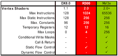
Obviously all of the features of the DX9 VS2.0 specification are support by the GeForce FX, and we've already highlighted some of the important ones here.
What you will quickly notice with the GeForce FX is that a lot of its advantages in pixel and vertex shader support will not be seen in games for at least another year, but more realistically 2+ years down the road. Remember that even Doom3 is built around more of a DX8 platform, with titles that would take advantage of these complex shader programs coming much later than next year. So on paper the GeForce FX will exert a number of these sorts of advantages over the Radeon 9700 Pro, but in the end they will not contribute to the overall performance of the card in the immediate future.
NVIDIA's got 8 pipes too
Just as we mentioned in our technology preview of ATI's R300, most DX9 based architectures will feature 8 rendering pipelines. The GeForce FX is no exception to the rule and it implements a virtually identical set of 8 128-bit floating point pixel rendering pipelines.
These fully floating point pipelines are where the majority of the GeForce FX's transistor budget is spent, but they are also what make the cinematic quality effects (or FX, if you will) possible. Once again, we've already explained the benefits of floating point color here.
Just like the Radeon 9700 Pro, the GeForce FX can only process one texture per pixel pipeline in a single clock, giving the GeForce FX no inherent fill rate advantage over the Radeon. NVIDIA makes up their performance advantages in their memory architecture, higher core clock speeds and overall efficiency. The GeForce FX, like the Radeon 9700 Pro, can process 16 textures per pixel, just not in a single clock which is often misunderstood.
Once again, NVIDIA went above and beyond the DX9 specification for pixel shaders and introduced what they call their Pixel Shader 2.0+ support. The advantages here continue to be in support for more instructions in shader programs among other things:
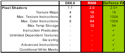
And once again we see that the GeForce FX part is more of an enabling product, with the real demand for end users to have this sort of "beyond PS2.0" support not arriving until at least a year from now.
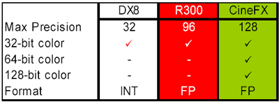
GeForce FX also supports greater color precision than any
competing product
Intellisample Technology: NVIDIA Strikes Back
Virtually everything up to this point has been NVIDIA more or less following the DirectX 9 spec and delivering what we have already seen from ATI. Granted, the GeForce FX does offer some enhancements in both the pixel and vertex shader categories but neither of those are going to be tangible to end users anytime soon. What will make games like Doom3 run faster however are things like NVIDIA's Intellisample technology.
Intellisample is NVIDIA's all encompassing term for their new color compression engine, improved fast z-clear, dynamic gamma correction, adaptive trilinear and anisotropic filtering, and anti-aliasing.
The first and most interesting of all of the new features is NVIDIA's color compression engine; the color compression engine sits between the rendering pipeline and the memory controller and compresses everything that comes out of the rendering pipeline before it is sent to memory. The lossless compression algorithm can obtain up to a 4:1 compression ratio which explains where NVIDIA gets their 48GB/s of memory bandwidth from. Remember that the 500MHz DDR2 memory on the GeForce FX provides 16GB/s of bandwidth on the 128-bit memory bus, but multiply that by 4 (don't forget to subtract out the original 16GB/s of data) and you'll get the 48GB/s of memory bandwidth NVIDIA is claiming.
It turns out that the compression engine is most useful when enabling anti-aliasing, and the reasoning behind this is simple; with conventional rendering you're taking one sample per pixel, and the color of that sample is rarely perfectly identical to that of adjacent samples. However, when anti-aliasing is enabled the GPU is taking multiple samples per pixel of identical colors which obviously compresses perfectly. The only time you don't get perfect compression is when you are sampling around the edges of polygons (vs. the interior of polygons).
The end result of this compression engine is that anti-aliasing now becomes a very low cost operation, since very little memory bandwidth is wasted. Essentially the only memory bandwidth used is on the edges of polygons, which make up a much smaller percentage of a scene than everything else. This should sound quite familiar as the results are similar to what Matrox promised (and delivered) with their Fragment Anti-Aliasing technology - only anti-aliasing the edges of polygons - however the difference is that there are no compatibility problems with NVIDIA's approach as it is still conventional multisampled AA.
The compression engine is completely invisible to the rest of the architecture and the software running on the GeForce FX, which is key to its success. It is this technology that truly sets the GeForce FX apart from the Radeon 9700 Pro.
The compression engine and the high clock speed of the GeForce FX enabled NVIDIA to introduce to new anti-aliasing modes: 6XS under Direct3D, and 8X AA under both OpenGL and Direct3D. Because of the compression engine, performance with AA enabled should be excellent on the GeForce FX.
Switching gears a bit, the GeForce FX also has a new, more efficient algorithm for clearing the Z-buffer. Known as Fast Z-Clear to those familiar with ATI's HyperZ technology, the GeForce FX basically has an improved version of the Fast Z-Clear that was in the GeForce4. The GeForce FX can also perform a fast color clear of the frame buffer but that is much less useful than fast z-clear.
On the topic of texture filtering, NVIDIA finally offers a non-purists anisotropic (and trilinear) filtering algorithm. This driver selectable option will enable users to choose from an accurate filtering algorithm (similar to what the GeForce4 currently has) or a slightly less accurate but very high performance algorithm (similar to what the Radeon 9700 Pro uses). The end result is that the performance hit incurred when enabling anisotropic filtering or even trilinear filtering when in this "performance" mode is considerably less. NVIDIA claims that their anisotropic filtering algorithm is more precise than ATI's, so the GeForce FX's anisotropic filtering should look just as good if not better than the Radeon 9700 Pro's.
FX Flow - Cooling the Beast
The first thing you'll notice about the GeForce FX is that the reference board takes up a total of two slot cutouts on the back of your case. The reason behind this is NVIDIA's FX Flow cooling technology that looks to be a combination of ABIT's OTES and eVGA's ACS2 technology, although NVIDIA did not license it from either of the aforementioned companies.


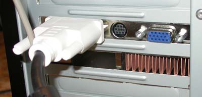
The cooler takes in cold air from the outside of the case, uses it to remove heat from the heatpipes that run around the GPU and memory devices (on one side of the PCB only) and finally exhausts the air outside of the case. The obvious benefit of this design is that the GeForce FX contributes very little heat to the inside of your case, but the clear downside is that the card occupies two slot cutouts.

NVIDIA has hinted at offering another version of the GeForce FX at a lower clock speed that would only occupy a single slot cutout, but we will have to wait until the product line is announced before we can find out what the differences will be. Our initial guess would indicate that a simple reduction in clock speed would be enough to go with a more conventional cooling setup.

The other issue that users may have is noise, luckily NVIDIA has taken steps to make sure that the GeForce FX is one of the most quiet running cards they've ever produced. Borrowing technology from their mobile parts and combining it with the FX Flow cooling system, NVIDIA is able to dynamically reduce the speed of the fan based on the graphical needs of the system. When sitting in a 2D situation the card will scale back the clock speed of parts of the 3D pipeline that aren't in use, thus allowing the fan to spin much slower. As soon as you start using the GPU for games or any other 3D intensive applications, the clock speeds up as does the fan. The idea is that if you're gaming you're not as concerned with noise as when you are typing in Word.
NVIDIA's FX Flow technology supports a wide range of speed levels to run the fan at; at its loudest the fan is no louder than a noisy Ti 4600.

Just like ATI's Radeon 9700 Pro, the GeForce FX will require a HDD/FDD power connector to operate. If you fail to connect a power cable the card will still work, just at a lower speed and it will display an error on your screen.
Performance
Interestingly enough, NVIDIA did not make many performance numbers available to us prior to the GeForce FX announcement. In fact, the majority of the performance numbers won't be revealed until after this article is published. Right now NVIDIA is claiming a 30 - 50% performance advantage over the Radeon 9700 Pro across the board. We will be able to put those claims to the test as soon as we have a card in hand.
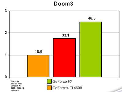
NVIDIA provided us with Doom3 scores that indicated a 40% advantage over the Radeon 9700 Pro.
When?
As we've mentioned before, the kicker is that the GeForce FX won't be available until February of next year. The chip itself is done and production is ramping up at TSMC; one of the causes for the delay is that producing the 0.13-micron wafers apparently takes several more weeks at TSMC than the older 0.15-micron process.
With availability in February, we're hoping to have review samples before the end of this year. As far as pricing goes, you can expect the fastest GeForce FX to be more expensive than the Radeon 9700 Pro. The real question is how much the "single slot" version will go for and how it will stack up to the Radeon.
Final Words
The launch of the GeForce FX reminds us a lot of the GeForce3; the GPU is impressive and it can enable a good deal of developers to make some great looking games, but it won't be out for a while and neither will those great looking games.
The perfect example we like to use is Doom3; Doom3 was designed around DX8 technology, it will be Doom3's successor that can truly take advantage of the features of GeForce FX. This is why we're not easily sold on advanced pixel and vertex shader support when it comes to GPUs; luckily NVIDIA was able to pack much more into the GeForce FX in order to make it quite attractive.
NVIDIA's Intellisample technology is the perfect example of the type of innovation we're used to seeing from them. NVIDIA will undoubtedly make the move to a 256-bit memory interface eventually, but until then the combination of high speed memory and their compression engine make for a very efficient use of memory bandwidth.
So there you have it; the elusive NV30 has surfaced in the form of GeForce FX. ATI has won the first round with the Radeon 9700 Pro, what will be most interesting will be what ATI has up their sleeves when the GeForce FX hits the shelves in February.