|
| ||
Three times's a charm, but what about the fourth?When the GeForce3 was released, NVIDIA wowed the press and end-users alike. They did so not with benchmarks or extremely high frame rates, but with the promise of enabling much greater reality in games. This lends us to the classic chicken and the egg syndrome when it comes to 3D graphics. Developers aren't going to spend time incorporating features such as DirectX 8 pixel and vertex shaders into their games unless the vast majority of the market has hardware capable of supporting such features. At the same time, the hardware will never make it out to the market if the vendors aren't producing it with the knowledge that end-users will essentially be paying for features they won't use for maybe even two years. Luckily both ATI and NVIDIA have provided the necessary hardware to make that a reality and now they're both on a quest to outfit the vast majority of the market that is still running on pre-GeForce3 platforms with better cards. The overall recommendations for the GeForce3 were that the technology has promise but there was no reason to purchase the card upon its release because of a lack of games that demand that sort of power. Fast forwarding to today, there's still no compelling reason to have the power of a GeForce3 however with NVIDIA's introduction of the GeForce3 Ti 200 it doesn't make sense not to have a GeForce3. The beauty of the GeForce3's introduction was that it was brought to market alongside a brand new API by Microsoft, DirectX 8. This gave the features that the GeForce3 touted much more credibility since they would definitely be used in games going forward. The launch of the GeForce4 isn't as blessed as DirectX 9 still lies in the somewhat distant future. The task on NVIDIA's hands is to make the GeForce4 as attractive as possible with other tangible features to convince the world to upgrade. It's up to you to decide whether the features are worth it, and it's up to us to present them to you. The GeForce4 core, as we've mentioned before, has been using the codename NV25 on all NVIDIA roadmaps. Architecturally, the core is quite impressive, as it is approximately 5% larger than the NV20 core while built on the same 0.15-micron process; keep that in mind as we go through the improvements the NV25 offers. First and foremost, as it was pretty much expected from the start, the NV25 now features two vertex shader units akin to the Xbox's NV2A GPU. The presence of two vertex shader units will help in games that make extensive use of vertex shading operations as they are inherently parallel in nature. As developers grow more ambitious with lighting and other vertex processing algorithms, the need for fast vertex shader units operating in parallel will increase. In the end both the pixel shader and vertex shader units will need to increase in performance in order to avoid any pipeline bottlenecks but you can expect to see the performance of pixel shaders improve tremendously while the future performance of vertex shaders will improve only a few fold over what we have today.
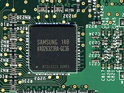
As you can see from the above picture of the NV25 core, the second vertex shader unit occupies a decent portion of the GPU's die. Just by visual estimation we'd say that the second vertex shader is around 6.25% of the GeForce4's die. Going back to the first thing we said about the NV25 core, the fact that it's only 5% larger than the NV20 core becomes that much more impressive. The pixel shader unit remains unchanged as does the majority of the rendering pipeline. The core still features 4 pixel pipelines and is capable of processing two textures per pixel; because of the core's programmable nature, it is possible to enable single pass quad-texturing just as was the case with the original GeForce3. NVIDIA's marketing name for the original set of pixel and vertex shader units of the GeForce3 was the nfiniteFX engine. The successor found in the GeForce4 is thus named nfiniteFX II and basically consists of the addition of a second vertex shader. Although we haven't mentioned clock speed yet, it should be mentioned that both the vertex shaders and pixel shaders operate at higher clock speeds as well in the GeForce4. The vast majority of the performance improvements of the NV25 core come from what NVIDIA is calling their Lightspeed Memory Architecture II. Before we get to what's new about LMA II let's talk about what's borrowed from the GeForce3.
This brings us to a new feature of the NV25's LMA II - NVIDIA's Quad Cache. With so much going on in the CPU world, you should already understand the need for efficient and high performance caches in any processor (graphics included). The Quad Cache is NVIDIA's name for the NV25's primitives, vertex, texture and pixel caches. The names of the four caches clearly explain their purpose in the GPU; the primitives and vertex caches store triangle data while the texture and pixel caches store texture and pixel data respectively. Not much is known about the size of these caches or how they've changed from those that were present in the GeForce3 but they are worth mentioning. It should also be mentioned that these types of caches aren't exclusive to the NV25 as the Radeon 8500's core has a similar set of caches. The reason caches play a much smaller role in the discussion of GPUs than they do in the CPU world is because they are not nearly as large of a portion of a GPU's core as the L1 and L2 caches are on most CPUs. Remember that today's GPUs run much slower than their memory busses while today's CPUs run 2 - 16 times faster than their memory buses thus making cache a much more important part of a CPU than of a GPU. Lossless Z-buffer compression is present in the NV25 core seemingly unchanged from the GeForce3. As you'll remember from our technology overview of the GeForce3, z-buffer data (data that indicates how "deep" in the screen or far away an object is from the user) is actually very easily compressible. Using a lossless compression algorithm, meaning that once uncompressed the data's values will be identical to their original form (much like zip file compression), NVIDIA is able to attain up to a 4:1 compression ratio on z-buffer data. Since a great deal of memory bandwidth is used by z-buffer reads and writes (the z-buffer is read from whenever a pixel is drawn), this compression can improve memory bandwidth utilization significantly. This is unchanged from the original GeForce3 core and a similar feature is present in all Radeon cores. Fast Z-clear also makes its way from the original GeForce3; this technology, also found in the Radeon cores, is an ultra-fast algorithm that is used to set all of the values in the z-buffer to zero. Why would you want to do that? After rendering a scene, the z-buffer values are no longer of any use for the next scene and thus must be discarded. By far the biggest improvement in the NV25's architecture that more than justifies calling it the 2nd generation Lightning Memory Architecture are the improvements in the Visibility Subsystem. The original GeForce3 introduced a feature that is known as Z-occlusion culling, which is essentially a technology that allows the GPU to look at z-buffer values in order to see if a pixel will be viewable when rendered. If the pixel isn't viewable and will be overwritten (or overdrawn) by another pixel, then the pixel isn't rendered and memory bandwidth is saved. This addresses the problem known as overdraw and in the NV25's architecture the performance of the Z-occlusion culling algorithms have been improved tremendously. While NVIDIA vaguely states that "LMA II increases fill rates by optimizing the read, write and selection of pixels to be rendered" this is one of those cases when reality is understated by marketing. You'll get to see the performance data behind this in the test section, but the GeForce4, clock for clock, is approximately 25% more efficient at discarding unseen pixels than the GeForce3. The final feature of LMA II is what is known as auto pre-charge. Remember that unlike cache, DRAM is capacitance based and thus must be refreshed in order to retrieve data from a DRAM cell. The benefit of this is that DRAM can be manufactured using far fewer costly components than cache but the downside being that there are sometimes hefty delays in getting access to information. One of those such delays occurs when attempting to read from or write to a part of memory other than the current area being worked with. What auto pre-charge does is it uses a bit of logic in the memory controller to effectively guess at what rows and columns in the DRAM array will be accessed next. These rows and columns are then charged before they are used thus reducing the amount of time that the GPU will wait if it does end up requesting data from the precharged rows/columns (banks). Should the GPU not request data from those banks then business is as usual and nothing is lost. Auto pre-charge in addition to the NV25's Quad Cache are very necessary in preventing the GPU from wasting precious clock cycles in an idle state, waiting for data from memory. Auto pre-charge won't offer more memory bandwidth directly however it will offer lower latency memory accesses which does in turn translate into a greater percentage of useful memory bandwidth. |
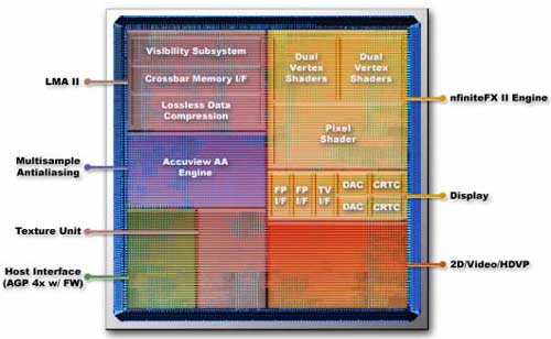
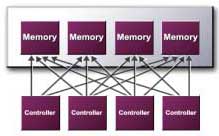 NVIDIA's crossbar memory architecture is still
present from the GeForce3. The architecture dictates that the GPU be
outfitted with not one but four independent memory controllers, each with
their own dedicated 32-bit
NVIDIA's crossbar memory architecture is still
present from the GeForce3. The architecture dictates that the GPU be
outfitted with not one but four independent memory controllers, each with
their own dedicated 32-bit
Accuview AAWe owe quite a bit to the late 3dfx, including some of the very first introductions to the world of true 3D gaming on our PCs. One thing that we most definitely have to "thank" 3dfx for is exposing us to anti-aliasing. After 3dfx demonstrated their VSA-100 architecture running current generation (at the time) games with FSAA enabled, we were spoiled for life. Suddenly we began picking out aliasing in virtually every game we saw, even first person shooters where aliasing wasn't supposed to be that big of a deal since everything was moving so quickly were victim to our obsession with FSAA. Unfortunately, the hardware available back then wasn't powerful enough to allow for FSAA to be enabled on most games. Finally, two years later, are we getting hardware that can run not only the present generation titles but as you'll soon see, the next-generation of games at high resolutions, at high frame rates, with AA enabled. Going back to that picture of the NV25 core you'll notice that almost 13% of the die is dedicated to what NVIDIA calls their Accuview AA Engine. When you're dealing with a part that's as complex as the NV25, dedicating such a large portion of the die to a single feature must mean that the feature carries great importance in the eyes of the manufacturer. In this case it's clear that NVIDIA's goal is to not only offer AA as an option to everyone, but to make it as much of a standard as 32-bit color depths. What the Accuview AA engine allows the NV25 core to do is have higher performance AA, even to the point where Quincunx AA can be performed at exactly the same speed as 2X AA. The new AA engine also allows for a new 4X AA mode only under Direct3D applications called 4XS. The difference between 4X and 4XS is that the latter offers more texture samples per pixel in order to generate a better looking AA image. |
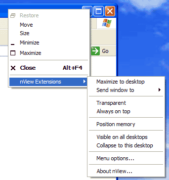
nViewOne of the most useful features of the NV25 core is the inclusion of the nView multiple display core. Originally introduced alongside the GeForce2 MX as TwinView, nView is an extension of TwinView with much greater flexibility from a hardware standpoint. The NV25 core features dual 350MHz integrated RAMDACs thus allowing for dual CRTs without any external circuitry. Although the core itself doesn't feature any TMDS transmitters there is support for up to two external TMDS transmitters on the GeForce4 to drive dual digital flat panel displays.
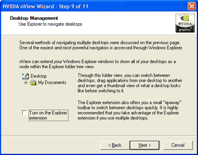
The hardware behind nView enables the technology but it is the software that exists that truly makes it a feature. From a software standpoint, NVIDIA managed to hire talent from the same company that ATI gained a lot of its Hydravision technology from - Appian. The end result is that nView is virtually identical to Hydravision in terms of features, but NVIDIA has made it slightly more user friendly by integrating a very simple 11-step setup process that can have any user up and running in as few as 11 clicks. The wizard clearly explains all of the major nView features and offers options to turn on/off features like multiple desktops.
Alongside the easy to use setup there are some other neat features that give nView the slight feature edge over ATI's Hydravision. For example, nView has a feature that allows you to set a double right-click to open a HTML link up in a new IE browser window on the second monitor. This is perfect for surfing websites or discussion forums so you can keep the main page open while opening an article or thread on the second monitor just by doubleclicking.
There are still features that both nView and Hydravision lack that give Matrox the slight leg up on both technologies but after using nView and Hydravision extensively for the past couple of weeks we can honestly say that NVIDIA has done an excellent job with nView on the GeForce4. |
The GeForce4 Titanium LineupWe've taken you this far without mentioning a single product based on the NV25 core, and now we're going to talk about just that. Today the GeForce4 is being introduced in two distinct flavors, the Titanium 4600 and the Titanium 4400. As was the case with the various GeForce3 Titanium cards, the two differ only in their GPU and memory clocks.
The 325MHz memory clock gives the Ti 4600 an incredible 10.4GB/s of raw memory bandwidth which is greater than the previous bandwidth champ, the Radeon 8500 with 8.8GB/s of bandwidth. Also keep in mind that these bandwidth figures aren't taking into account efficiency improvements such as through LMA II on the GeForce4 or HyperZ II on the Radeon 8500. |
 The GeForce4 Ti 4600 is NVIDIA's new flagship and
will feature a 300MHz core clock. The card will also feature a
128-bit
The GeForce4 Ti 4600 is NVIDIA's new flagship and
will feature a 300MHz core clock. The card will also feature a
128-bit