Presented by: Only On Saturday Night
IdeZilla Circuit Boards
TTL
GARAGE WORKBENCH
PIX
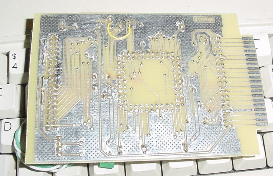
Here's the back side, not much to see.
Three jumpers set address ranges:
$FF00-$FF08
$FF10-$FF18
$FF20-$FF28
$FF30-$FF38
$FF40-$FF48
$FF50-$FF58
$FF60-$FF68
$FF70-$FF78
One more jumper allows the "extra registers":
$FF09-$FF0A
$FF19-$FF1A
$FF29-$FF2A
$FF39-$FF3A
$FF49-$FF4A
$FF59-$FF5A
$FF69-$FF6A
$FF79-$FF7A
Addresses form $FFXB to $FFXF are unused and not activated.
One more jumper inverts the register sets.

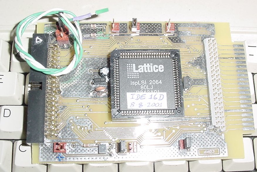
Top view.
The seven jumpers seen (each jumper has two positions) set addresses,
etc.
The three on the right are set for inverted register set (A0, A1 &
A2).
The four on the left are set to $FF6X, (A7, A6, A5 & A4).
Address line A3 used internally, to select between CS0 and CS1.
Very short 40-pin cable connecting the "edge connector" to the "board".

Closer up version, shows the chips used.

Back Side. Shows how the front edge connector is layed out.

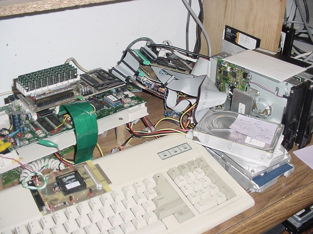
"Hand" View. Shows actual size, not very big.
This circuit board has an adapter attached as the connector. It requires a short cable connector on this board to work, ie strap both headers together, this could be done with insulated wire staples. This adapter can be cut loose and used to extend this main board to another location, i.e. farther away. The main board can be used separately to connect to the "bottom header", here on this site. The cable that would be the extention cable will have it's rows swapped, this is OK! This board is made for this row swapping, especially if someone uses that "bottom connector" scheme.
Address Ranges: Using Jumpers JA4, JA5, JA6 and JA7. Corresponding directly
to address lines A4 to A7.
$FF00-$FF08
$FF10-$FF18
$FF20-$FF28
$FF30-$FF38
$FF40-$FF48
$FF50-$FF58
$FF60-$FF68
$FF70-$FF78
Any bytes past $FFx8 are unused and not activated. So, bytes from $FFx9
to $FFxF are free and unused.
Oh by the way, each IDE drive is partitioned to 6 major partitions. Each partition has 261,888 sectors, DMODE shows cyl=03FF, sid=08, sct=20. This gives about 18 logical drives. /DD, /MD1, /MD2, /MD3, /MD4, /MD5, /SD0, /SD1, /SD2, /SD3, /SD4, /SD5, /I0, /I1, /I2, /I3, /I4, /I5. /MDx is part of the "master" on that cable, /SDx is the "slave" drive on the same cable, /Ix is the test drive getting "filled up". There is a separate driver for each IDE drive, so for this setup there's three IDE drivers (besides all of the /xx descriptors). The "fun" part is when I try to find where I was the last time I assembled the current drivers, etc.
How about plugging more ide-cards & drives ? (still have 2 more) <grin>. Sounds like a RAID setup, no? I would've loved to have this setup back when BBS's were popular.
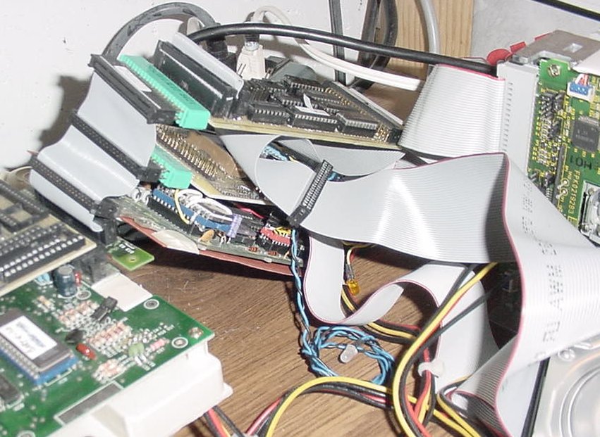
Shows another view of that "plug-in" stack. You can see the "MPI"
cable plugging into the coco game port with one of those hacked "PC" edge
connectors, wired to plug in directly. The 64MB interface has 74BCTxxx
CPU address & RW buffers, enough to drive this "cable". I may
change over to 74ACxxx drivers as they allow "+50ma/-50ma" output drive.
You'll notice that there's only two of those "green" card-edge connectors
in the cable. The floppy card has gold-pins soldered on top of those old
oxidized edge fingers, much more reliable this way.
There's that second CPLD IDE interface laying on the XT keyboard.