|
|
Robert Gault's Notes
My Notes
Downloads
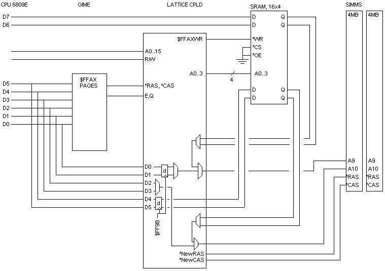
SRAM Drawing
VidTest: (6309)
VidTest8: (6809)
MemTest: (6309)
MemTest8: (6809)
The BIN files are RS-DOS Binary Executable files. (RS-DOS = Tandy Disk
Basic, CoCo-3 Style)
LOADM"VIDTEST/BIN:0" : EXEC
The ZIP files have both ASM and BIN inside.
Use OS9 DOS command to move files from a PC to a pre-formatted OS9 or
NitrOS-9.
In a DOS window type: OS9 A: -put vidtest.bin vidtest.bin
Use the OS9 RsDos command to move from OS9 or NitrOS-9 to a pre-formatted
RS-DOS floppy.
RsDos -put -m /d0 VIDTEST.BIN vidtest.bin
| VidTest.BIN
VidTest.ASM VidTest.ZIP MemTest.BIN MemTest.ASM MemTest.ZIP |
| VidTest8.BIN
VidTest8.ASM VidTest8.ZIP MemTest8.BIN MemTest8.ASM MemTest8.ZIP |
| os9202.zip
os9206a.lzh |
| Turbo_2.a |
| BARTONLY.BIN
Bart.BMP |
| Date: Sat, 13 Nov 1999 23:16:12 +0000
Reply-to: Robert Gault <[email protected]> From: Robert Gault <[email protected]> Subject: Re: 8MB NoCan3 Testing, seems complete. To: [email protected] On Paul's system, each MMU address selects a standard $2000 block of RAM. Since the MMU registers are 8 bit lines they only address $FF*$2000 or $1FE000. The address needs to be extended for two more bits at $FF9B to get $400*$2000 or $800000. Here is how I would describe the system. 1) The video bits (xxmmvvvv) at $FF9B have immediate effect and are used in conjunction with the video offset registers $FF9D-$FF9E. The combined registers create a pseudo 20 bit register. This enables access to 1,048,576 (2^20) video offset locations. Since the offsets are separated by 8 bytes, this covers 8* 2^20 = 8,388,608 (8Meg). 2) The memory bits (xxmmvvvv) at $FF9B have no effect until a value is sent to an MMU register, $FFA0-$FFAF. When a value is sent to an MMU register, the memory bits at $FF9B combine with the MMU register to create a pseudo 10 bit register. This enables access to 1024 (2^10) MMU blocks for a total memory of 1024*8192=8,388,608 (8Meg). 3) The value at $FF9B is latched and therefore stable but is write only as are the two high bits in the MMU registers. Paul is able to run OS-9 Level II on the system, but I believe he needed to change the manner in which the memory bits were processed. There are more details on his web page describing how to keep the DRAM at $xFExx constant. It was a real challenge to write code for this
system without having the hardware for testing. However, the programs were
valuable as they permitted Paul to determine that two bits of the Lattice
CPLD schematic were reversed. Reprogramming resulted in contiguous memory
as indicated by the Vidtest program.
"L. Curtis Boyle" wrote:
|
| Date: Wed, 29 Dec 1999 22:27:44 +0000
Reply-to: Robert Gault <[email protected]> From: Robert Gault <[email protected]> Subject: Re: What's New? To: [email protected] Being a diehard Cocoist, I obtained an 8 Meg board from Paul T. Barton ( the second production unit I believe.) While installation is not for the timid, all went well and I now have an 8 Meg Coco3 which can run at 4 MHz using a 63B09. I have chosen to stay with standard clock speeds for now. I am pleased to be able to recommend the high
quality of the NoCan3 PC board and report that Paul has done a superb job
with his project. Without making any changes to my NitrOS9 software, the
new system reports 2 Meg memory. My RGB-DOS hard drive ROM Basic system
is also happy with the new hardware.
|
| This 8MB interface is just
an extension to the already existing 2MB interface.
A 2MB interface is not needed,
this board emulates the original 2MB interface.
For NitrOS-9 users, no changes are required to use the 2MB. For OS9 users, you must patch the system for the 2MB to be useable. |
| $FFA?
-------- 76543210 |||||||| |||||||`---- MMU bit 0, immediate ||||||`----- MMU bit 1, immediate |||||`------ MMU bit 2, immediate ||||`------- MMU bit 3, immediate |||`-------- MMU bit 4, immediate ||`--------- MMU bit 5, immediate || |`---------- 1mb bit 6, immediate (CPU) 1MB `----------- 2mb bit 7, immediate (CPU) 2MB Test Video Memory (8MB): This is immediate. 1. Write page # to $FFA?, lower
6 bits only.
1. and 2. are not sequence dependant, 2 can be executed before 1. Sequence:
Or:
|
| $FF9B
-------- 76543210 |||||||| |||||||`---- bit 0, immediate (Video) 1MB ||||||`----- bit 1, immediate (Video) 2MB |||||`------ bit 2, immediate (Video) 4MB ||||`------- bit 3, immediate (Video) 8MB |||| |||`-------- bit 4, sequenced to SRAM (CPU) 4MB ||`--------- bit 5, sequenced to SRAM (CPU) 8MB || |`---------- nc `----------- nc Test CPU memory (8MB): This is sequence dependant! Only $FF9B bits 4 & 5 are
sequence dependant,
1. Write page bits to $FF9B,
bits 4 and 5 only.
As the $FFA? pages are used,
Sequence:
|
| NOTE !!
This is a text for you to use to study the capabilities of the CoCo-3. Some minor parts may be in error (??), and some info is not shown. (Tandy insiders should clue us in on these, and other capabilities.) Purpose of release is to show some of the extra thought in the machine. In NO way should it be construed as an "official map". Now have fun! -- Kevin * Thanks from all of us to the many contributors who shall remain unknown! * -----------------------------------------------------------------------------
SYSTEM MEMORY MAP:
64K PROCESS MAP:
Note: the Vector Page RAM at 7FE00 - 7FEFF,
when enabled, will appear instead
XFF00-0X PIA0
(not fully decoded)
FF90 INITIALIZATION REGISTER 0
CoCo bit set = MMU disabled, Video address
from SAM, RGB/Comp Palettes = CC2.
FF91 INITIALIZATION REGISTER 1
FF92 IRQENR Interrupt
Request Enable Register (IRQ)
I have no idea if both IRQ &
FIRQ can be enabled for a device at same time.
FF94 Timer MSB
Write here to start timer.
FF96 reserved.
FF98 Alpha/graphics Video modes,
and lines per row.
FF99 VIDEO RESOLUTION REGISTER
Text: CoCo Bit= 0 and FF98 bit7=0. CRES0 = 1 for: attribute bytes are used.
HR2 HR1 HR0 (HR1 = don't care for text)
---------------------------------------------
X Colors HR2 HR1 HR0 CRES1 CRES0
512 4 - 1 1
0 0 1
320 16 - 1 1
1 1 0
Other combo's are
256 16 - 1 1
0 1 0
160 16 - 1 0 1 1 0 Old SAM modes work if CC Bit set. HR
and CRES are Don't Care in SAM mode.
FF9A Border Palette Register (XX00
0000 = CoCo 1/2 compatible)
FF9C Vertical Fine Scroll Register
If Bit 7 set & in Text mode, then
there are 128 chars (only 80 seen)/line.
FFA0-AF MEMORY MANAGEMENT UNIT
(MMU)
If you don't know what a DAT or MMU is, read CCRAM.TXT in DL6 of OS9 SIG. Each register has 6 bits into which
is stored the block number 0-63 ($00-$3F)
MMU Register:
CPU:
-------------------------------------------------------------------
A- 18 17 16 15
14 13 12 11 10 9 8
7 6 5 4 3 2
1 0
Taking address bits 18-13, we have:
0 1 1 0 1 0, or $1A, or 26. This is the
Now, let's say you'd like to have that
block appear to the CPU at Logical
You would store the Physical Block Number
($1A) in either of the two Task Map
To find the address within the block,
use Address Bits 12-0 plus the Logical
FFB0-BF COLOR PALETTE REGISTERS
(6 bits each)
Reg bits- 5 4 3 2
1 0
When CoCo Bit is set, and palette registers
preloaded with certain default
40/80 Column Text Screen Bytes are
Even=char, Odd=attribute, in memory.
Char Attributes- 8 bits... F
U T T T B B B
FFC0-DF SAM : same as before (mostly
compatible Write-Only Switches)
|