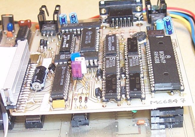
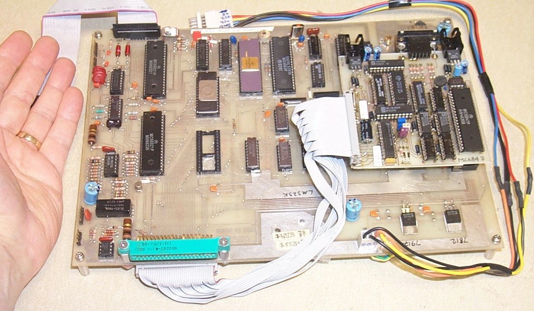
It also has a plug-in board that converts the 6847 analog levels to
CGA. I suppose that it could be converted to VGA too. The circuitry is
basically an op-amp driving a ladder string of resistors tied to the inputs
of a lot of very fast comparators. These comparator outputs then go to
a PAL for the color conversion. Then these signals go through an SRAM for
the Color-Look-Up-Table and then through buffers and out to the CGA connector.
Buffers exist for the sync signals, VSYNC and HSYNC. I plugged this board
into my newly acquired Tandy CM-5 and it works great!
The only challenge is that the Graphics Green
and the Text Green are the same and cannot be separated, that is the way
that the 6847 works. All other colors are separate. With this CGA device,
you are not stuck to a fixed 4-color scheme for games, etc. The colors
can be any of the eight colors available. The intensified bit is also used
(Yellow uses it, Orange doesn't, same color otherwise) and available as
data input. So, you have the eight colors in CGA with 7 more intensified.
For instance, Black (no I bit), bright Black (I bit used), dim White (no
I bit) and White (I bit used). Also, Dim and Bright, Blue, Red, Magenta,
Cyan, Green.
| Color to Change | Address | Data Binary RGBI | Data Decimal RGBI | Data Binary RGBI Intensified | Data Decimal
Intensified RGBI |
| Green | 0 | 0100 | 4 | 0101 | 5 |
| Yellow | 1 | 1101 | 13 | 1101 | 13 |
| Blue | 2 | 0010 | 2 | 0011 | 3 |
| Red | 3 | 1000 | 8 | 1001 | 9 |
| Buff | 4 | 1110 | 14 | 1111 | 15 |
| Cyan | 5 | 0110 | 6 | 0111 | 7 |
| Magenta | 6 | 1010 | 10 | 1011 | 11 |
| Graphics Orange | 7 | 1100 | 12 | 1101 | 13 |
| Graphics Black | 8 | 0000 | 0 | 0001 | 1 |
| Text Orange | 9 | 1100 | 12 | 1101 | 13 |
| Text Black | A | 0000 | 0 | 0001 | 1 |
| Sync (Black) | B | 0000 | 0 | 0000 | 0 |
The Color-Look-Up-Table is loaded as follows,
Poke the SRAM c-l-u-t address with
nibble of SRAM address bits and nibble of SRAM data bits, merged together
into one byte:
POKE &HFF80,&HAD REM AD= clut address(A), clut data(D).
Defaults:
POKE &HFF80,&H04 REM address 0 data &H4
POKE &HFF80,&H1D REM address 1 data &HD
POKE &HFF80,&H22 REM address 2 data &H2
POKE &HFF80,&H38 REM address 3 data &H8
POKE &HFF80,&H4E REM address 4 data &HE
POKE &HFF80,&H56 REM address 5 data &H6
POKE &HFF80,&H6A REM address 6 data &HA
POKE &HFF80,&H7C REM address 7 data &HC
POKE &HFF80,&H80 REM address 8 data &H0
POKE &HFF80,&H9C REM address 9 data &HC
POKE &HFF80,&HA0 REM address 10 data &H0
POKE &HFF80,&HB0 REM address 11 data &H0