TABLE OF CONTENTS
List of figures
List of tables
2.4 Voltage Control Oscillator
2.7 Digital to Analog Converter
2.8 Impedance Matching Network
3.2.1 Frequency Down Conversion
6. Conclusion and Recommendations
Appendices
Appendix A AM MATHAMATICAL EXPRESSIONS 28
LIST OF FIGURES
Figure 2.1. Example of an AM signal
Figure 2.2. Block Diagram of a Heterodyne
Figure 2.3. Block Diagram of Phase Lock Loop
Figure 2.4. Matching 1500ohms to 50ohm at 10Mhz using tapped-c network.
Figure 2.5. Simulation Results of the Impedance Matching Network
Figure 2.7. Simulation Result of the 25dB Attenuator Pad
Figure 3.1. Block Diagram of the System
Figure 4.1. Layout of VCO
Figure 4.2. Schematic of the band-pass filter
Figure 4.3. Schematic of the low-pass filter
Figure 5.1. Spectral View of the Mixer Output.
Figure 5.2. Simulation results of the band-pass filter
Figure 5.3. Simulated results of the low-pass filter
Figure 5.4. Schematic of a 25dB Attenuator Pad
LIST OF TABLES
Table 4.1. List of Components
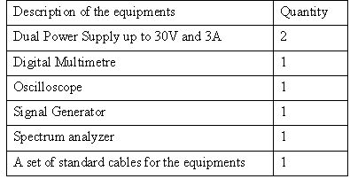
Table 4.2. List of Test Equipment
CHAPTER 1
Currently, the area density of magnetic data storage technology is increasing
at an annual rate of 80-120%. Finding the height between the read/write head
and the disk plates becomes more critical, with an expected increase of area
density to 200Gb/in2. Reduction of the magnetic spacing is inevitable from currently
25nm to a possible of 10-12nm.
There are different methods of finding the flying height between the read/write
head and the surface of the disk plate. DSI (Data Storage Institute) has come
out with a new/modified method to calculate the flying height between the read/write
head and the surface of the disk plate.
For this method, the amplitudes of the read back signal and its harmonics are
required. These read back signals are sort of like AM signals. The amplitude
of the signal is directly affected by the flying height between the read/write
head and the surface of the disk plate. A fixed disk plate with uneven surface
will cause a change in amplitude of the read back signal. The frequency of the
amplitude change depends on the spinning speed of the disk plates. A change
in amplitude constantly of a fix pattern (if it test over the same track with
a constant spin and the height of the disk plate) simulates a signal with a
characteristic of an AM signal. It has a modulating signal of 1kHz - 200kHz,
modulated by a carrier signal equivalent to the test frequencies. When carrying
out signal testing, in order to pick out the desired signals within different
bands, a large number of band-pass filters/demodulators with the corresponding
central frequencies will have to be designed.
1.2 RATIONAL
To find the amplitude of the harmonics of the read back signals, a number of
band-pass filters/demodulators were needed for corresponding test frequencies.
This makes the job tedious, impractical and a waste of resources. Measurement
prototypes for this purpose do exist but none has the ability to cover a wide
range of frequency bands.
The objective of this project was to build a demodulator that is able to handle
an input AM signal with a bandwidth of about 400MHz. The expected output of
the test board will be the modulating signal. This signal must be extracted
without much distortion. The operation of the test board is preferably PC controlled
or automated.
The first phase of this project was to identify and gather the necessary components
required, and to configure them to the specifications of the project.
The second phase of this project will be to build the prototype, and carry out
research and development to further improve on the prototype. This includes
implementing PC control and interface.
This prototype should be able to demodulate the read back signal over a wide
range of frequency (10MHz to 400MHz) to certain accuracy. The prototype should
also be PC controlled.
By the end of the first phase, all components required should be consolidated
and successfully configured. Each stage of the prototype should be configured
to match corresponding stages.
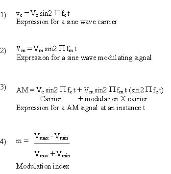
Modulation is the process of modifying the characteristic of one signal (carrier
signal) in accordance with some characteristic of another signal (information
signal). Information signal varying the amplitude of the carrier signal is know
as amplitude modulation (AM). It means that the instantaneous value of the carrier
amplitude changes in accordance with the amplitude and frequency variation of
the modulating signal.
For this project, the modulating signal (information signal) is generated by
the hard disk, which has a frequency ranging from 1-200KHz with an approximate
of 100mVp-p with the carrier signal range from (10-400) MHz. Modulation depth
or modulation index is the ratio of the modulating signal voltage to the carrier
voltage. The modulating signal voltage must be less than the carrier voltage
for a non-distort AM signal. The AM generated by the hard disk has a modulation
depth of 10-15% for normal cases and up to 30% for worst cases. Refer to Appendix
A for the Mathematical representation for AM and the formula for modulation
depth.
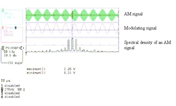
Figure 2.1. Example of an AM signal
2.2 HETERODYNE
Heterodyne is a process whereby a modulated signal frequency is changed to a
higher or lower frequency without affecting the integrity of the information.
This is done by mixing the modulated signal with another signal (preferably
a pure sine wave) in a non-linear device such as the diode mixer. The output
of the mixer will be the sum and difference of the input signal frequencies.
This is also known as IF (intermediate frequency). There are other signals present
at the output of the mixer, such as the input signals and the multiples of the
IF. This project will be using an IF of 10MHz. Thus, the difference's of the
inputs is selected by using a band-pass filter.
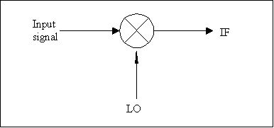
Figure 2.2. Block Diagram of a Heterodyne
2.3 PHASE LOCK LOOP (PLL)
PLL has three basic parts, a phase detector, a low-pass filter and a voltage
control oscillator. It has two inputs and an output. PLL is an electronic circuit
that controls an oscillator so that it generates a constant phase angle and
frequency relative to a reference signal. Phase detector compares the two AC
input signal and produce a DC output call the error signal. The low-pass filter
that comes after the output of the phase detector is to remove other frequency
other than the DC error signal. Which is use to control the VCO which in turn
feedback to one of the input of the PLL.
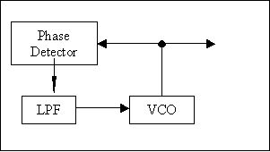
Figure 2.3. Block Diagram of Phase Lock Loop
2.4 VOLTAGE CONTROL OSCILLATOR (VCO)
VCO is an electronic circuit that generate a pure signal of a certain frequency
and amplitude. The frequency generate by the VCO is dependent on the DC control
voltage and the amplitude is dependent on the power supply to the VCO. However
there are limits to both the frequency and amplitude of the signal. These are
dependent on the circuit design. There are two main types of VCOs, linear and
non-linear tuning VCO. Linear tuning VCOs have their frequency changes linearly
in accordance to the control voltage. The non-linear tuning VCOs have their
frequency changes exponentially in accordance to the control voltage.
Low-pass filter is a network or device that passes all frequencies below a specified
frequency, known as the cutoff frequency, with little or no loss, but reduces
the power of higher frequencies greatly.
Band-pass filter is a network or device that ideally passes all frequencies
between two non-zero finite limits and bars all frequencies not within the limits.
2.7 DIGITAL TO ANALOG CONVERTER
Converting a digital signal to an analog signal, one needs to use a digital
to analog converter. Digital signals in the form of binary are being decoded
to a set of decimal values. The range and resolution of the decimal values depend
on the type of DAC being use and how it is configured.
2.8 IMPEDANCE MATCHING NETWORKS
2.8.1 Tapped-C Network
Impedance matching networks are used to join two networks or circuits with different
impedance together. This is to allow maximum power transfer between the two
networks or circuits, thus increasing the efficiency of the overall networks.
Tapped-c network is a narrow band impedance matching network, which employs
the use two series capacitor in parallel to a capacitor and inductor. Below
is a schematic of the network at 10MHz with the simulated result.

Figure 2.4. Matching 1500ohms to 50ohm at 10Mhz using tapped-c network.

Figure 2.5. Simulation Results of the Impedance Matching Network.
2.8.2 Attenuator pad
The main purpose of the attenuator pad is to reduce the power of the signal
by a specific value. However, it can also be use in impedance matching between
two networks or circuits. The whole network uses only resistors thus it is possible
to operate over a wideband of frequencies. Refer to appendix B for the formulas.
CHAPTER 3
PRODUCT DESCRIPTION
The demodulator is built on PCB board, measuring 297mm in length by 210mm in
breadth and 1.4mm thick. The material of the PCB is FR 4 with a dielectric-constant
substrate of 3.2. The traces on the PCB board are 0.6mm wide. Each pad on the
board measures 1.9mm in diameter and the holes are 1mm in diameter. The surface
mount devices are mounted on the topside of the PCB, and the other components
are soldered onto the other side. The four corners of the PCB are fitted with
metal support. Each support is 20mm in length and 2.5mm in diameter.
3.2.1 Frequency Down Conversion
First, the PC will generate an 8-bit data, which is sent to the DAC (Digital
to Analog Converter). The DAC will convert the 8-bit data into a voltage level,
which controls the VCO (Voltage Control Oscillator) so as to produce a signal
10MHz lower than the hard disk's read back signal. Both the read back signal
and the signal produce by the VCO are passed into the mixer. The mixer will
produce the sum and difference frequencies of the two signals. A band-pass filter
with a center frequency of 10MHz and a bandwidth of 400kHz is use to select
the difference frequency at the output of the mixer.
The 10MHz read back signal will then be demodulated using coherent detection.
First, the signal is passed into a PLL (Phase Lock Loop). The phase detector
will generate a signal, which goes through a loop filter, to control a VCO with
a frequency range that covers 10MHz. The signal generated by the VCO will be
looped back into the phase detector, which will compare the frequency and phase
of both signals, and adjust the control signal accordingly, such that the signal
generated by the VCO will be identical to the carrier of the read back signal.
Both the signals from the band-pass filter and the VCO are then passed into
another mixer. Since the two signals are identical phase, by selecting the difference
signal at the output of the mixer with a low pass filter, the 10MHz carrier
of the read back signal will be removed. This leaves only the modulating signal,
which is 1kHz - 200kHz with minimum phase distortion.
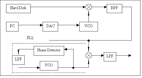
Figure 3.1. Block Diagram of the System
3.3 HOW TO USE IT
First, the interface between the PC and the prototype has to be set up by connecting
a cable between the PC's parallel port and the parallel port of the prototype.
Next the respective VCO is selected for testing by setting the jumper. The prototype
is then powered up. Link up the read back signal from the DUT (Device Unit under
Test) to the prototype through a 50ohm cable.
Execute a program name "Flying height variation test". Proceed with
the instruction stated in program to continue the testing. Once the parameters
are input into the program, it will process and have the necessary data output
to the prototype through the parallel cable. Have a oscilloscope hook up at
the output to monitor the output signal.
CHAPTER 4
PRODUCT DEVELOPMENT
4.1.1 RESEARCH
In general, the project can be broken into two main stages. First is to solve
the problem of filtering out a small spectrum of signal from 10-400MHz with
a constant bandwidth of 400KHz. Second is to demodulate the filtered signal
with little or no error.
Books and the Internet were researched and some possible solutions were found.
First possible solution would be the use of switch capacitors in a filter design.
At different frequency, the capacitance can be adjusted thus adjusting the center
frequency of the filter across the band. However the bandwidth may vary at different
center frequencies. In order to have a fixed bandwidth, the other components
will also have to be variable. This method is impractical as such a filter will
not be user friendly. Second design is based on the theory of heterodyning.
That is to reduce the modulated signal to a fixed IF (intermediate frequency)
and use a band-pass filter to pass only the IF (for the theory of heterodyne
refer to chapter 2). Although there are other possible solutions, these two
is the simplest of all. For flexibility and simplicity reasons, the second design
was selected.
There are two way of detecting the modulating signal, coherent and non-coherent
detection. Removing the carrier frequency from the modulated signal by mixing
through a mixer does coherent detection. Therefore the carrier frequency must
be known before hand. Non-coherent detection is the simplest of all but in most
cases this method affects the integrity of the signal. Phase shifts, which affect
the integrity of the signals, have to be taken into account as well. Thus coherent
detection is use to fulfill the project requirements. This will involves the
use of a PLL to generate the carrier signal with similar phase compared to the
modulated signal.
4.1.2 DESIGN
Most of the components used were SMD (surface mount device) IC (integrated chip).
Therefore, data sheets and applications notes were refer to configure the ICs
to perform the operation need in the prototype. To ensure that the configuration
is correct, test boards were built to test the ICs configuration. If the output
of each testing matches the expect results, it would mean that the IC suits
the project.
There were other parts such as filters and attenuator pads had to design from
scratch. Research was made to find the correct formulas need to design those
circuits. Calculations were made and prepared for the using of simulating software
to verify the results. Microwave Office version 4.0 was the software used for
simulating the results. By simulating the results from calculation, it would
not only verify the results, optimization operation could also be perform so
as to reduce the time and resource to build and test circuits through try and
error method.
When all was done, all the different stage is integrated together to form the
whole prototype. Later, testing was done on the prototype. The first integration
was not very successful because of the poor design of the PCB and the lack of
understanding between different networks. Subsequently, improvement were made
through further understand, testing and consultation.
4.2 COMPONENT SELECTION
To reduce the size of the overall prototype, most of the components are surface
mount devices (SMD). The important factors that affect the selection of the
components are bandwidth operating frequency range. Most of the components had
to be either wideband or high speed.
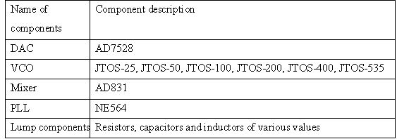
Table 4.1. List of Components
4.3 FABRICATION & ASSEMBLY
Test boards were built for each of the components required. Protel 99 second
edition was used for schematic and printed circuit board (PCB) design. Upon
completion, the designs for the PCB was printed in negative and sent for fabrication.
The process of the fabrication is known as wet process, which involves the use
of chemicals to remove the unwanted copper on the substrate.
Once the PCB is ready, soldering of the components can be done. As stated earlier,
most of the components are surface mount thus the traces of the PCB needs to
be tinted manually. These ease the mounting of SMDs. Throughout the assembly
stage, care and cautions were taken when comes to mounting the SMDs ICs onto
the PCB because there were limited amount of ICs due to detail planning of budget
usage.
At the beginning, possible components were selected for the project. Although
data sheet of each component can be found stating the characteristics, testing
needs to be done on most components to know if it is suitable for the project,
and to configure it to suit the requirements of the project. Some were found
to be too difficult to configure while others were just not suitable due to
its physical dimensions or it's characteristics. Each time a testing is done,
a set of standard equipments is required. A list is complied in a table below.
4.4.1 VCO
Since the VCO used is a SMD, a PCB had to be fabricated for testing.
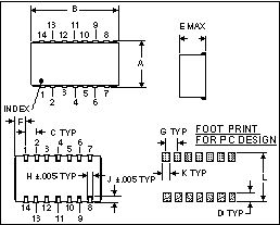
Figure 4.1. Layout of VCO
A 12V power supply was connected to pin 2, and the tuning voltage was connected
to pin 5. This tuning voltage controls the output frequency of the VCO, which
can be monitored using an oscilloscope or a spectrum analyzer by tapping at
pin 13. The remaining pins were grounded.
A test board was fabricated to test the mixer. A 5V and -5V power supply and
ground was connected to power up the circuit. All the power supplies are DC
coupled and the mixer is configured to produce a 10dB gain. Signal generators
were used to simulate the input signals to the RF input and the LO signals through
SMA ports. The output of the mixer is monitored on a spectrum analyzer.
4.4.3 Band-Pass Filter
The band-pass filter was designed using lump components like resistors, capacitors
and inductors. After the necessary components were calculated, a simulation
was done using MWO. Further simulations were performed to archive realizable
component values.
The circuit is then built on a vero-board and tested using a network analyzer.
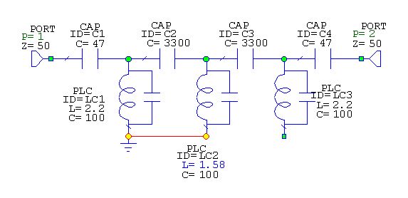
Figure 4.2. Schematic of the band-pass filter
4.4.4 Phase Lock Loop
A test board was fabricated to test the PLL. A 5V power supply and ground was
connected to power up the circuit. Signal generator was used to simulate the
input signals to the input at pin 6. The output of the PLL, pin14, was monitored
on a spectrum analyzer.
Like the band-pass filter, the low-pass filter was built using lump components.
After the necessary components were calculated, a simulation was done using
MWO. Similarly, further simulations were done to obtain realizable component
values. The circuit is then built and tested using the network analyzer.
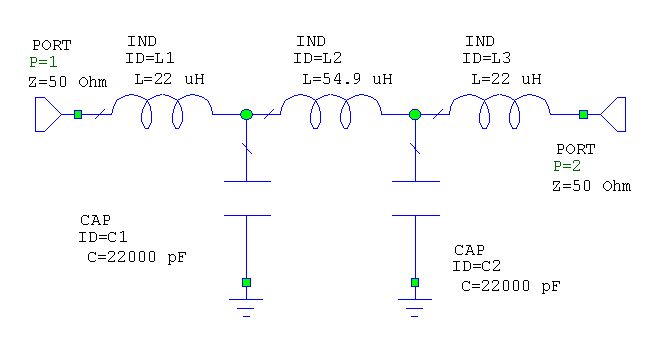
Figure 4.3. Schematic of the low-pass filter
4.4.6 Attenuator Pad
Component values for the attenuator pads were calculate and simulated using
MWO. After obtaining the values, by performing optimization, a circuit is built
according to the design. Testing is further done on the circuit.
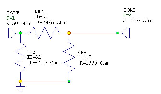
Figure 5.4. Schematic of a 25dB Attenuator Pad
4.5 FINAL PRODUCT IMPROVEMENT
At this stage, only components had been selected for integration of the entire
prototype. However, there could be some improvement to be made such as to select
a cheaper but of the same quality components, components of properties to reach
a higher operating frequency at the first stage of the prototype, frequency
down conversion. These would reduce the cost of the prototype if it were to
be mass produce and with a bonus of higher operating frequency.
Although the design of the prototype is up but there is still room for improvement
such as to increase the sensitivity by adding a pre-amplifier at the input.
CHAPTER 5
RESULTS AND DISCUSSION
5.1.1 VCO
The VCO was able to produce an output signal varies from 8 - 10dB, depending
on the range of the model of the VCO and the tuning voltage. However, it was
discovered that there is a slight drift of the output frequency respective to
the corresponding tuning voltage as given in the data sheets. But this problem
can easily be overcome as the tuning of the VCO is done manually. The tuning
voltage can be adjusted accordingly to produce the desired output frequency.
The mixer was able to produce the sum and difference frequencies of the RF input
and LO signals. It could produce a 10 dB gain as it was configured to.
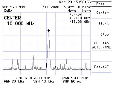
Figure 5.1. Spectral View of the Mixer Output.
5.1.3 Band-Pass Filter
The simulated result produced by MWO gives a pass-band attenuation of almost
0dB, and 3dB cut off frequency at 9.82MHz and 10.2MHz, giving a bandwidth of
about 400KHz. It had a reflection coefficient of -33.8dB.
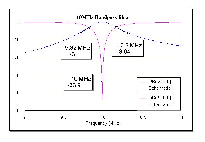
Figure 5.2. Simulation results of the band-pass filter.
Practical result, however, showed an attenuation of about 3dB at the pass-band
of 10MHz. This could be due to cable losses or drift in component values at
high frequencies. But this result is still acceptable.
5.1.4 Phase Lock Loop
The PLL could produce a signal of the same frequency as the input signal. It
has a slight distortion and phase shift, but these were negligible.
5.1.5 Low-Pass Filter
The simulated result produced by MWO gives a pass-band attenuation of almost
0dB, and 3dB cut off frequency at 262kHz, and a reflection coefficient of -19.6dB
at 20kHz.
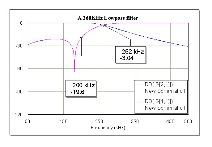
Figure 5.3. Simulated results of the low-pass filter.
After testing with the network analyzer, it was discovered that the filter
has a pass-band attenuation of about 3dB. This problem can be easily overcome
by configuring the amplifier to have a certain gain to make up for the filter's
loss.
Throughout the six months, we manage to get hold of the necessary components
through numerous literature survey and individual component testing. Doing literature
survey was not easy for us because of the broad area we had to cover. We had
to carry out a numerous researches for various components needed, such as the
mixers and PLLs.
Some of the components originally selected were later found to be unsuitable
for the project due to certain properties that were overlooked initially. Testing
of selected components was delayed because of purchasing time, which could take
up to three weeks.
Besides testing of components, we had to design various circuits like the filters
and the attenuator pads. These circuits were designed and simulated using Microwave
Office (MWO) version 4.0. Numerous optimizations had to be made to the pre-calculated
values using MWO to achieve realizable values.
The second phase of the project will be continued next semester. This includes
building the complete prototype by integrating the individual stages together,
and setting up a PC control and interface.
We have learned many things throughout the course of this project. Through
literature surveys, we learned theories and circuit designs related to RF (Radio
Frequency). We also gained a better understanding of practical circuit design,
building and testing.
CHAPTER 6
CONCLUSION AND RECOMMENDATIONS
The objectives for the first phase of this project have been met, which is to
identify and gather the necessary components required, and to configure them
to meet the specifications of the prototype.
Some improvements can be made to the project, such as catering for a wider range
of frequencies. This can be done by including additional VCOs to generate higher
LO frequencies, and using a mixer with a higher bandwidth.
The sensitivity of the prototype can also be improved by adding an amplifier
before down converting the read back signal. However, only a linear amplifier
can be used so as not to have any distortion to the signal. Also, it would be
best to be able to adjust the gain of the amplifier in order to produce a -10dB
signal, the level at which the mixer performs best.
1. Louis E. Frenzel, Communication Electronic principles and application, McGraw-Hill,
Singapore,2000.
2. E.da Silva, High frequency and microwave engineering.
3. Delton T. Horn, Design and building electronic filters.
4. William F. Egan, Frequency synthesis by phase lock loop.
5. Vadim Manassewitsch, Frequency synthesizer Theory and Design, John Wiley
and Sons, New York,1987.
1) Data sheet for VCO JTOS-100, Minicircuits, 2001, < http://www.minicircuits.com/cgi-bin/vco?model=JTOS-100&pix=bk276.gif&bv=4
>, (August to December)
2) Phase lock loop fundamentals, Minicircuits, 2001, < http://www.minicircuits.com/appnote/vco15-10.pdf>,
(August)
3) VCO test method, Minicircuits, 2001, < http://www.minicircuits.com/appnote/vco15-15.pdf>,
(August)
4) AD7528, Analog Devices, 2001, < http://products.analog.com/products/info.asp?product=AD7528>,
(August)
5) AD831, Analog devices, 2001, < http://products.analog.com/products/info.asp?product=AD831>,
(August)
6) NE564, Philips semiconductor, Philips, 2001, < http://www.semiconductors.philips.com/pip/ne564n>,
(August)
7) SA605, Philips semiconductor, Philips, 2001, < http://www.semiconductors.philips.com/pip/sa605d>,
(August)
8) SA612, Philips semiconductor, Philips, 2001, < http://www.semiconductors.philips.com/pip/sa612ad>,
(August)
9) CLC111, National semiconductor, National, 2001, < http://www.national.com/search/search.cgi/main?keywords=CLC111>,
(August)
10) 74F164A, Fairchild semiconductor, 2001, < http://www.fairchildsemi.com/pf/74/74F164A.html>,
(August)
11) "Slot Seven" Tunable Inductors, Coilcraft, 2001, <http://www.coilcraft.com/slot7.html>,
(August)
1) B. Liu and Z. M. Yuan, "In-Situ Characterization of Head Disk Clearance",
Heads, Media & Materials / Failure Analysis & reliability / Contamination
Analysis & control, vol. 1, pp. 37-46, 2000
2) Z.M. Yuan, B. Liu, Q.F. Leng and Q.S. Chen, "Scanning Carrier Current
Method for In-Situ Measurement of Flying Height Variation", Heads, Media
& Materials / Failure Analysis & reliability / Contamination Analysis
& control, vol. 1, pp. 71-76, 2000
APPENDIX A AM MATHAMATICAL EXPRESSIONS