 |
 |
 |
| Home:> VLSI Experiences |
| Very Large Scale Integration (VLSI) circuit technology is an enabling technology for implementaion of highly integrated complex systems. Involvement of VLSI designer with knowledge and expertise of VLSI design process technology will impact archtectural trade off's and help in realization of the best architecture. |
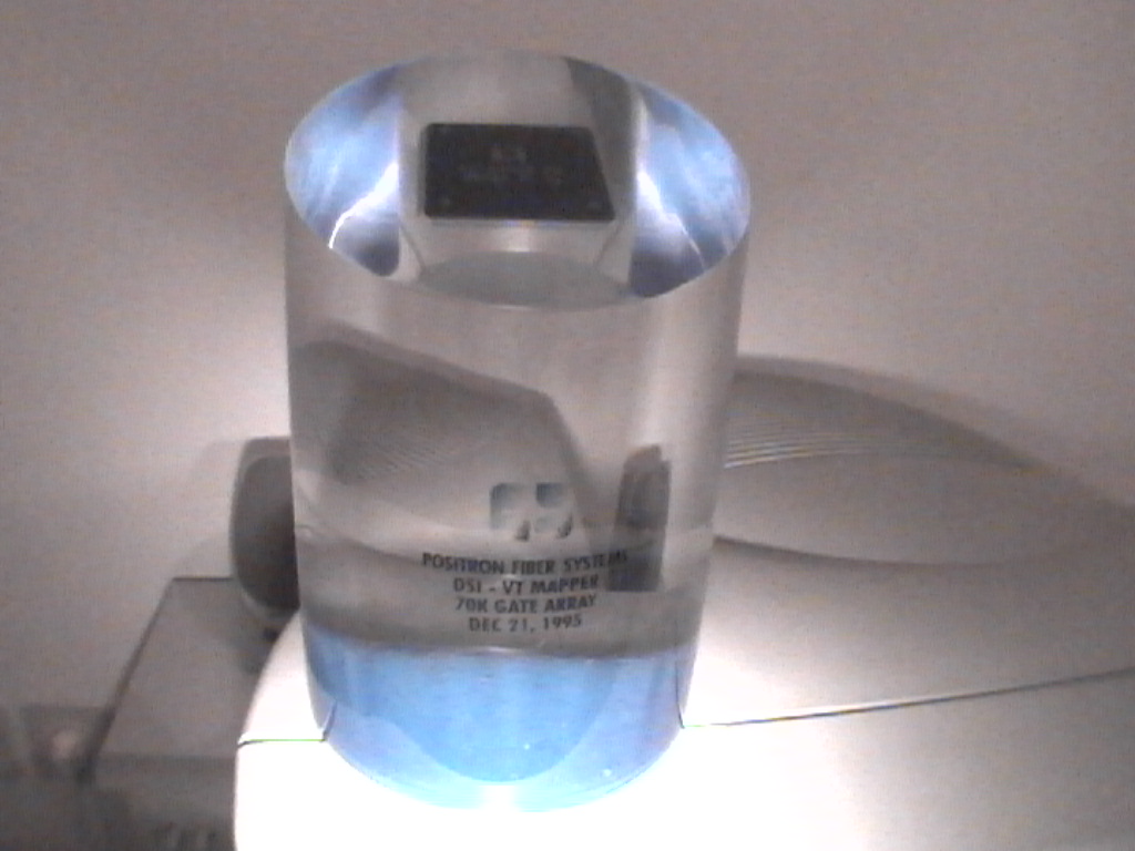
| Converted an FPGA designs into a Custom-IC. The FPGAs design, mapps/demapps DS1 trafiics into/fromSONET payload. (Mapping DS1 traffics into VTs and finaly into OC-3 SONET payload, and demapping VTs from SONET payload into DS1 traffics). The goal was cost reduction. |
Prior to joining to VLSI group, I worked in a very complex FPGA designs, such as bridges between PCI and UTOPIA buses, MVIP interfaces to communicate custom ASICS with Texas Instrument DSPs. |
| For each integrated circuit designed, test vectors are developed by the VLSI design team to assure a supply of high quality and reliable device. The minimum stuck at one and zero fualt coverage of these vectors are required to be 95%. In order to make this goal achievable partial scan and/or full scan test schemes is used. This approach will allow for application of Automatic Test Vector Generation (ATVG) tools and reduce test vector generation time. This test methodology will make high fault covergae required achievable. |
| The goal of all VLSI development is to realize first-time success in a timely fashine. High Level design methodology is the design methodology of choice for VLSI design. This Methodology requires RTL design and algorthmic mapping of the specification using VHSIC Hardware Description Language (VHDL), and RTL simulation and verification of the design in the context of the system. Once the design is described in VHDL and verified, combination of logic synthesis and manual logic design process will be used to decompose and map the design into an integrated circuit technology. |
| Go to: Home |
| An optical interface ASICs for OC-48/OC-12 Broadband Transport Manager System, Tellabs Operation Inc. |
| I was a member of VLSI group (15 engineers) who designed In house Custom-IC for various Tellabs Projects. For the last two years we had developed an optical interface ASIC for OC-48 Tellabs Broadband Transport Manager System. I was responsible for RTL design development, chip level functional verification, synthesis and timing analysis. |
| Five Years in Service at Tellabs Operation Inc. Worked in three different projects. |
| Go to: Home |
| Dec. 21, 1995, An award given to me from POSITRON FIBER Systems. My carrier started with this 70K gate array in which FPGA designes are integrated for cost reduction. The design had first-time success, with few minor bugs. |