 |
| Foto album of nano electronic laboratory tour |
|
 |
 |
 |
 |
 |
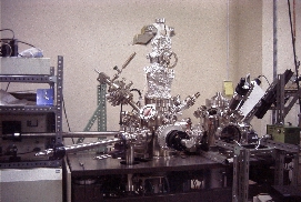
| EFM (Exchange Force Microscope) |
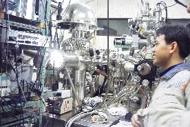
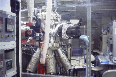
| STM (Scanning Tunneling Microscope) |
| Back |
| Top |
| More |
 |
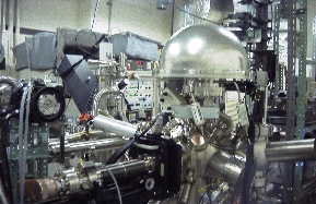
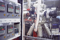
| MBE (Molecular Beam Epitaxy) |
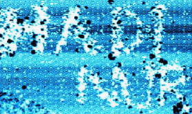
| STM images of field emission induced surface modification of a word �gHadi Nur�h on a Si(111) 7�~7 reconstructed surface. Writing on a flat terrace by applying a continuous negative voltage pulse of 4.2 V for 0.1 ms. The image has a scan size of 45�~75 nm2. |