| IDE interface - Introduction | ||||||||||||||||||||||||||||||||||||||||||||||||||||||||||||||||||||||||||||||||||||||||||||||||||||||||||||||||||||||||||||||
| Introduction | Register selection | IDE interface | Commands | | ||||||||||||||||||||||||||||||||||||||||||||||||||||||||||||||||||||||||||||||||||||||||||||||||||||||||||||||||||||||||||||||
|
I had a problem of storing
data with quick accessibility some time ago and I had the idea of using a
hard disk for that purpose. As a result I implemented this small
interface first to understand the operations of the IDE interface.
But I was in really trouble when trying to get the interface
details, how ever I managed to overcome those problems. So I put
this information to you so that you can implement your own
interfaces for hard disks with ease. Hard disk interface is a 40 pin connector where you can write or read two bytes at once. Although the hard disk is considered as a random access media, it can access only blocks of data (512 bytes) at once but not bytes as in memory modules. With the information that I have published here I think you can have a rough idea of the usage of this interface for your implementations. I must tell you that the controlling the hard disk is very simple as reading or writing data to or from memory module. |
||||||||||||||||||||||||||||||||||||||||||||||||||||||||||||||||||||||||||||||||||||||||||||||||||||||||||||||||||||||||||||||
|
|
||||||||||||||||||||||||||||||||||||||||||||||||||||||||||||||||||||||||||||||||||||||||||||||||||||||||||||||||||||||||||||||
|
40-pin connector interface signals
|
||||||||||||||||||||||||||||||||||||||||||||||||||||||||||||||||||||||||||||||||||||||||||||||||||||||||||||||||||||||||||||||
|
Introduction From a controller point of view an IDE interface could be described as a set of I/O ports. The IDE interface has a 8/16 bits I/O bus, two /CS lines, a /WR and /RD line, three address bits and one interrupt. In this description I assume the most traditional IDE interface. The data bus on an IDE interface is used mostly for 16 -bits transfers. When implementing a 16-bits I/O port all you need is a bidirectional I/O port and some control bits (8 bits at least) to generate the /RD, /WR etc... Pin description |
||||||||||||||||||||||||||||||||||||||||||||||||||||||||||||||||||||||||||||||||||||||||||||||||||||||||||||||||||||||||||||||
|
||||||||||||||||||||||||||||||||||||||||||||||||||||||||||||||||||||||||||||||||||||||||||||||||||||||||||||||||||||||||||||||
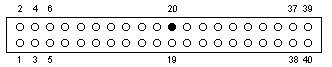 IDE
pin out diagram.
IDE
pin out diagram. 18th January 2003 - Pubudu Goonetilleke