|
|
||||||||||||||||||||||||||||
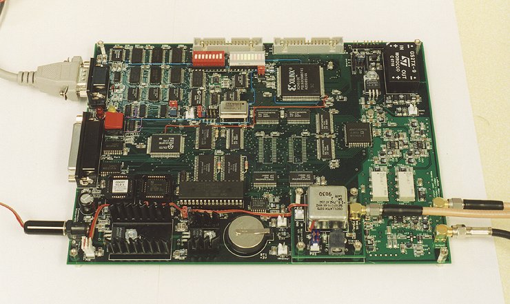
The transmitter was primarily designed for research and proof-of-concept
applications where new modulation and coding methods are tested.
The primary goal was to design a device as flexible as possible,
loaded with features necessary for experimentation, and built with
readily available components. It took me only 10 weeks from
the first touch of the schematic, through development and PCB design,
till the hand-soldered three fully functioning prototypes were ready
for demonstration.
|
| Power source |
7.5V .. 18V/0.9A DC regulated on board, 2.5mm power connector |
| I and Q channel resolution | 8 bits/channel |
| IF oscillator frequency | 25 .. 250MHz |
| IF oscillator power |
-3dBm .. +12dBm +5dBm recommended |
| IF oscillator leak |
>30dBc 36dBc typical |
| IF oscillator impedance | 50 Ohm |
| Output power | 0dBm typical |
| Output impedance | 50 Ohm |
| I/Q modulator | HPMX-2005 |
| I and Q modulator bandwidth | >40MHz typical |
| Antialiasing I/Q filters |
Fixed 21.4MHz or 10.7MHz cut off |
| Clock reference frequency |
1 .. 25MHz TTL levels Internal XCO or external signal |
| Maximum sampling frequency |
40-80MHz depending on DAC 40MHz with pulse shaping |
| Physical dimensions |
178 x 242 mm 7 x 9.5 inches |
![]()
Description
Bellow is a block diagram of the CPU part of the transmitter and the description of the different parts of the transmitter.
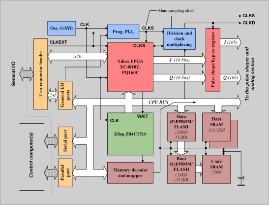
D/A converter, RF section, and I/Q modulator
The Analog Devices DAC 8-bits per channel is used for D/A conversion. The antialiasing filters are fixed and soldered on the board. The Hewlett Packard HPMX-2005 vector modulator is used for I/Q modulation. DC component in both I and Q branches are removed, so for example amplitude modulation cannot be generated, at least not directly, by the transmitter. The output is amplified to get typical output power of 0dBm.Pulse shaper
As a compromise between price, power consumption, and flexibility the fast SRAM implementation was chosen over the FIR or FIR in FPGA implementations. Two fast 128KB SRAMs are used as a pulse shaper. The Xilinx output, 16 bits/channel are connected to the SRAM address bus. All the possible pulse combinations must be stored in the SRAMs.Because only 64KB are used for pulse shaping per channel at a time, the user can prepare two pulse shaping alternatives per channel. The CPU controls the bank switching.
The data outputs of the memories are buffered and fed to the 8-bit DAC. For modulations without pulse shaping (rectangular pulse shape) the the whole pulse shaper section can be bypassed. Switching to the bypass is controlled by CPU and it is a default after the reset/power up. When the pulse shaper is bypassed, only the Xilinx I channel is used for modulation and is buffered and fed directly to the DAC.
Note that for some simple pulse shaping the Xilinx can be configured to do the job as well, chip space permitting.
Xilinx FPGA transmitter core
Xilinx XC4010E FPGA in PQ 160 pin package is used as a transmitter core. If more logic is necessary for the transmitter core the XC4020XL can be used, which has the same pinout in PQ 160 pin package.Clock generation
The generator of the sampling frequency (the highest used in the system) is a programmable PLL chip capable or delivering output frequency in between 391kHz to 100MHz. The input reference frequency for the PLL loop must be in the range between 1MHz and 25MHz.
The CPU clock and the PLL input clock can be independently connected to one of the signal sources:
-
Crystal socketed TTL oscillator on board.
Bi-directional header to which external clock
signal can be connected. If the header is configured
as output the internal crystal oscillator
output can be connected to it.
Using this configuration it is possible to synchronize:
- CPU clock with data sampling clocks.
- Data clock and/or CPU clock with the incoming data bit stream clock signal. One can either lock the incoming data stream to internal clocks or lock internal clocks to incoming data stream.
The output of the PLL is fed directly to Xilinx. The PLL output signal is also divided by 2 and connected to another input Xilinx clock pin.
There are two major clock signals going to the pulse shaper/DAC section. The pulse shaper or pulse shaper bypass register symbol clock CLKD and the DAC sample clock CLKS. Both signals can be independently generated by the following sources:
-
CLKD - Xilinx dedicated output XCLKD
or direct PLL output
CLKS - Xilinx dedicated output XCLKS
or direct PLL output
This clock schemes allows for wide range of combinations of CPU, symbol, and sample clock frequencies.
Embedded CPU
Zilog embedded controller on board with clock speed up to 16MHz is used. It integrates clock controller, wait signal controller, two parallel and two serial channels, and four counter/timer channels.Memory mapping
The following memory is on the board:-
32KB SRAM for boot/code - the CPU will run program in this memory - battery back-up.
1MB SRAM for data - battery back-up.
2x128KB fast SRAM for pulse shaper - not suitable for battery back-up.
32-pin DIP socket for data/boot code - possible EPROM, EEPROM, FLASH in 128KB, 256KB,
or 512KB sizes. The bottom 16KB of the memory can be configured to be the boot code
memory.
32-pin PLCC socket for data - possible EPROM, EEPROM, FLASH in 128KB, 256KB, or 512KB sizes.
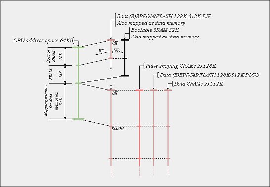
By a jumper setting a user can control whether the transmitter will boot from (E)EPROM/FLASH or from battery back-up SRAM. Switching between SRAM and (E)EPROM/FLASH is also possible by software. Special circuitry protects battery back-up SRAM during the power on/off transient periods. Bus request sliding switch and the reset button allows user to change the boot configuration jumper without turning the transmitter off.
If the CPU is running from (E)EPROM/FLASH, the writes to the code bottom 16KB locations will go to the underlying SRAM. This write-through topology allows for easier configuration and gives a user more freedom in utilizing the transmitter resources.
CPU and Xilinx interfacing
There are two major modes of interfacing between CPU and Xilinx and several levels of interfacing and synchronization can be used in each mode.- Xilinx is mapped to the CPU I/O space, both WR and RD. Total of 32 RD and 32 WR ports are available for internal Xilinx decoding.
- Two WR and two RD port control signals are decoded externally and fed to 4 Xilinx I/O pins for applications where FPGA chip space is critical.
- Xilinx can control CPU /WAIT signal for CPU/Xilinx synchronization, which is faster than port pooling.
- Part of the CPU is used as a fully programmable interrupt controller for Xilinx. There are two levels of maskable interrupt dedicated to Xilinx with fully programmable priorities.
- CPU non-maskable interrupt signal /NMI is fully controlled by Xilinx for fast responses.
- Xilinx controls (by open drain output) CPU bus request signal /BUSRQ and monitors /BUSACK.
- Full access to all of the transmitter memory.
- The CPU/Xilinx shared I/O port on the header H2 is used internally by Xilinx in DMA mode and in not available for I/O purposes in this mode.
- Full access to all on-board control and configuration ports.
- Full access to CPU on-chip ports. Xilinx FPGA can communicate with both serial and parallel ports on its own without CPU intervention. This can be especially useful for fast data transfer through the parallel port.
CPU is running
This mode is a normal operational mode when CPU is running and is not in DMA mode. Several methods of CPU/Xilinx interfacing include:
CPU is idle in a DMA mode
This mode is a special operational mode when Xilinx takes over busses and disconnects CPU from the resources. Xilinx can take over busses permanently or only temporarily if needed and then return control to CPU. It is totally up to the user what DMA feature are programmed into the Xilinx FPGA. Theoretically, the CPU does not have to be even soldered on the board. The whole transmitter can be operated in Xilinx DMA mode only. The Xilinx DMA mode features include:
Configuration jumpers and connectors
The transmitter hardware features following connectors and headers for configuration, communication, and expansion:- Serial RS-232 interface 9-pin DB-9 female connector.
- Parallel PC port connector 25-pin DB-25 female with the same pin numbering as on PC, but connected as receiver. Straight pin-to-pin DB-25 male-male cable must be used for connecting PC to the transmitter.
- Two SMA 50 ohm female connectors for IF oscillator input and transmitter output.
- Power DC connector with internal diameter 2.5mm, ground on
the sleeve.
- Header H1 - 34-pin header with 24 signal pins directly connected to Xilinx pins. There is also a digital ground and +5V at several places on the header for convenience.
- Header H2 - 34-pin header with one CPU 8-bin output and two 8-bit input ports. One of the ports is also directly connected to Xilinx pins. If Xilinx is in DMA mode, this port is used for addressing purposes and cannot be used by a user.
- Xilinx XChecker header - connector for the XChecker cable. If the
XChecker is not used some of the header pins can be used for general
input/output signals.
- Power headers - 2-pin polarized headers with power source voltages:
- Board input DC voltage, common ground.
- Digital +5V, digital GND.
- Analog +5VA, analog AGND.
- Analog -5VA, analog AGND.
- Clock input/output header - can be configured for both input and output. See the clock generation section for details.
- Clock configuration header - configures the clock source for CPU and PLL.
- Xilinx configuration header - it is used to set Xilinx control signals for different configuration methods.
- Control header - selects after-reset polarity of signals controlling boot memory and Xilinx programming.
- Memory selection headers - two 10-pin headers for each (E)EPROM/FLASH socket. Just two jumpers can select one of the EPROM, EEPROM or FLASH type of memories and one of the 128KB, 256KB, or 512KB sizes.
Software
As a first phase a comfortable firmware monitor was developed. It communicates over the RS-232 with speeds up to 57600Bd with standard speed 9600Bd. It features input line editor and remote echo, so any modem software featuring ANSI terminal can be used for communicating with the transmitter.
Monitor CMON
The monitor, CMON 1.17, is a terminal oriented basic communication software with command line interface and file download feature. The files can be send to the transmitter over the serial/parallel link in three different formats:- Intel HEX - Intel HEX format with 32bit address extension. Records of types 02H, 03H, and 04H are all considered to contain upper 16 address bits.
- ASCII HEX - format generated by some FPGA tools and DSP compilers. ASCII format without address specification where each binary byte is represented by two ASCII characters, similarly as in Intel HEX case. Bytes can be (but do not have to be) separated by spaces, new lines, or tabulators.
- Binary - binary format as-is without any additional address information.
The monitor features over 30 commands including:
-
SRAM memory operations - manual editing, read memory in ASCII HEX,
ASCII HEX with address for more readability, or binary, file download to memory in one
of the three formats mentioned above.
FLASH memory operations - FLASH manual editing, chip erase, multiple sector erase.
FLASH can also be programmed by sending file to the transmitter in the Intel HEX
or ASCII HEX formats.
Xilinx programming - programs Xilinx from any memory location, or downloads
the configuration to Xilinx directly in one of the three formats mentioned above.
It also features automatic /PROG jumper setting sensing.
Port operations - read, write, bit mask operations on some control ports.
Serial port speed setting - dynamic serial port speed setting.
Sample PLL clock setting - setting the PLL sample clock frequency from a command line
to any frequency in the PLL range.
Cold/warm start automatic sensing - distinguishes automatically between warm and cold
starts. Optional execution of user program during the cold start.
The user can also prepare configuration text file with monitor commands. Intel HEX or ASCII HEX data can be in the file as well. The file can then be sent to the serial port for batch configuration of the transmitter. The terminal software is not necessary in this case.