Fascinating world of space exploration. My interest in Space Shuttle is related
to one of the projects I designed:
Get Away Special Space Shuttle Experiment
I came to PennState University in summer 1992 and joined the Get Away Special (GAS)
Space Shuttle Experiment team at the Department of Electrical Engineering.
Several years before, what was then the aerospace division of General Electric,
bought 3 GAS canisters for PennState electrical engineering students to build
experiments for the Space Shuttle. In summer 1992 the second of the projects
was on the way and all the experiments were specified. I ended up designing
 Single Event Upset high density static RAM radiation experiment
that was ultimately flown on the Space Shuttle
Endeavor STS-77 on May 19, 1996.
The goal of the whole GAS experiment was to design 4 experiments to be flown on the space shuttle.
Finally, 3 experiments were flown. The one was involved tested high-density static RAMs for single
event upsets (SEU), also known as soft errors. When a high-energy particle (proton, for example) goes through
the semiconductor dice, it leaves energy trace behind it. In some cases the energy causes the flip of the
static memory flip-flop resulting in the change of the information originally stored. Because
the memory chip is not permanently damaged by that, therefore the name "soft error" is used comparing
to the "hard error" when the chip is permanently damaged.
Testing the memories for the SEU might look as a simple task. Write a predefined pattern to the
memory under test (MUT), wait some time, say 10 minutes, read the data back from the memories,
compare the read data with the data originally written, and store the location and value of the
upset to some permanent memory. Pretty simple task on the Earth. In the space environment,
the situation is more complicated, because the controller performing that "simple" task must
be fault-tolerant, because it is in the same hostile environment as the memories under
test. The design of such a fault-tolerant controller is no longer a simple and straightforward task.
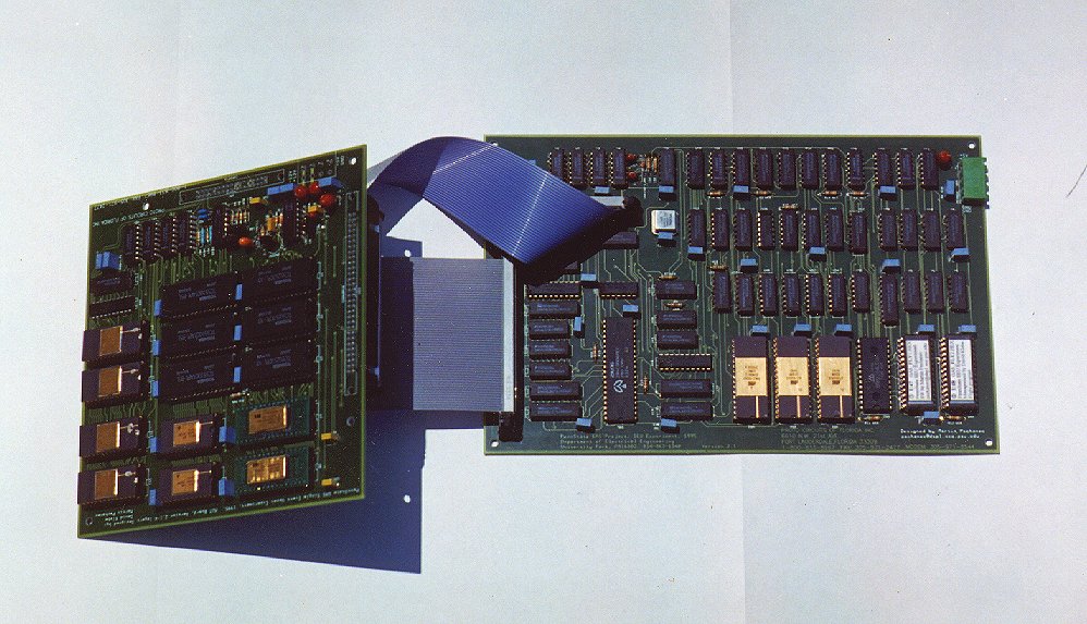
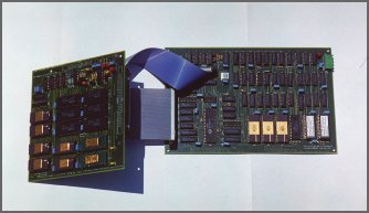
Fault-tolerant controller
The picture of the whole experiment is above. The bigger board on the right is the controller board
mounted inside the GAS canister. The smaller board on the left is the memory-under-test (MUT)
board, which was mounted just beneath the lid of the canister.
As mentioned above, designing fault-tolerant controller is a pretty tricky task. The main rules used for the
design were:
- Use bipolar technology as much as possible, because with 12 and more bipolar transistors per gate
in 54LS and 54ALS technology the bipolar technology is much less sensitive to SEU than MOS
technologies.
- Controller should be 8 bit microprocessor with the lowest clock frequency possible.
- Store the code in EPROM, but develop error-correction scheme to be sure, that partially
damaged memory will not trash the whole experiment. Because of floating gate in EPROM
storage MOS transistor cell, a high energy particle may change the charge in the floating
gate resulting in the permanent bit change.
- For retrieved data storage use EEPROMs along with some error-correction scheme to be sure read data
will not be damaged. Because the experiment was designed to run for about one week, the data
must be well protected.
- Because timing was critical, do not use any CMOS out-of-shelve clock chips, but use the chain of bipolar
counters as a time ticker and take care of the timing in software, storing the timer data
in EEPROM.
- Design the hardware and software such that if something fails the controller would be able to
recover from the failure, resume operation from the point where it crashed, and wrote to the
data EEPROM what happened and when.
- Several different patterns should be used for testing MUT.
- Develop a HW/SW write protection scheme, such that if the microprocessor loses the proper
program addressing (high-energy particle can go through the microprocessor sending it
to some unused code area), the stored data will not be damaged by accidental arbitrary writes.
The block diagram of the experiment is in the figure bellow.
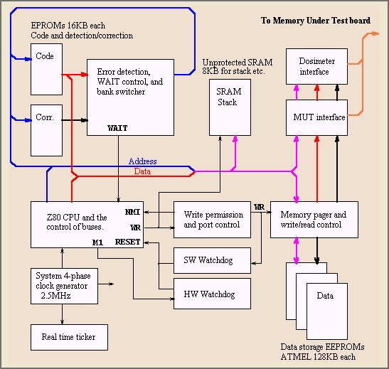
Description of different parts of the controller:
Z80 CPU, bus control and system clock generator
The CMOS version of Z80CPU was used as an experiment overall controller. Johnson counter was used to generate
4-phase system clock out of the 10MHz oscillator, so the microprocessor ran on 2.5MHz system clock.
Special care was taken to ensure proper bus timing and data bus buffer reversals were carefully controlled
by extra circuitry.
Error protection of the code
The code was stored in the CMOS 16KB EPROM memory. Inherently, as mentioned above, EPROMs are sensitive
to radiation. Because of the floating gate, we can end up with the permanent information change, so some
error correction is essential. Because of the low level design, error-correction codes
for actual real time code error correction were not used due to the hardware complexity of such a task.
Instead, error-detection scheme was used.
There was another EPROM along with the code one, carrying error-detection information. Two interleaved
extended systematic (8,4) Hamming codes were used for error detection. Both codes have the same generator
matrix G, which were algebraically manipulated to get the simplest possible realization
of the detection circuitry. The generator matrix for each of the codes was
for each of the codes
            1 0 0 0  1 0 1 1
        G = 0 1 0 0  1 1 1 0
            0 0 1 0  1 1 0 1
            0 0 0 1  0 1 1 1
such that the overall generator matrix for the (16,8) interleaved code was
            1 0 0 0 0 0 0 0  1 0 0 0 1 0 1 0
            0 1 0 0 0 0 0 0  0 1 0 0 0 1 0 1
            0 0 1 0 0 0 0 0  1 0 1 0 1 0 0 0
        G = 0 0 0 1 0 0 0 0  0 1 0 1 0 1 0 0
            0 0 0 0 1 0 0 0  1 0 1 0 0 0 1 0
            0 0 0 0 0 1 0 0  0 1 0 1 0 0 0 1
            0 0 0 0 0 0 1 0  0 0 1 0 1 0 1 0
            0 0 0 0 0 0 0 1  0 0 0 1 0 1 0 1
resulting in the parity matrix H in the form
            1 0 1 0 1 0 0 0  1 0 0 0 0 0 0 0
            0 1 0 1 0 1 0 0  0 1 0 0 0 0 0 0
            0 0 1 0 1 0 1 0  0 0 1 0 0 0 0 0
       H =  0 0 0 1 0 1 0 1  0 0 0 1 0 0 0 0
            1 0 1 0 0 0 1 0  0 0 0 0 1 0 0 0
            0 1 0 1 0 0 0 1  0 0 0 0 0 1 0 0
            1 0 0 0 1 0 1 0  0 0 0 0 0 0 1 0
            0 1 0 0 0 1 0 1  0 0 0 0 0 0 0 1
where the error control byte [c7 .. c0] is calculated from the actual code byte
by
-
[c7 c6 ... c0] = [d7 d6 ... d0] * G
and the syndrome, which should be zero, is calculated by the hardware as
-
H * [d7 d6 ... d0 c7 c6 ... c0]' = 0.
Such arrangement creates two interleaved codes, each having Hamming distance of 4,
therefore being able to detect 3 random errors. By interleaving we end up
with a (16,8) code capable of detecting a burst of 6 errors in a row, which
is the most probable scenario.
The main trick is that there are 4 identical copies of the code and the correction part
in both EPROMS. If microprocessors reads from the code EPROM, the hardware automatically
calculates the syndrome and checks is for zero. If there is an error in the code and/or
correction ERPOM, the syndrome is non-zero. The circuitry asserts WAIT signal to the CPU,
switches to another copy of the code, and checks again. If there is an error at the same
address in the next copy, it tries the third copy of the code. If it finds correct data,
it gives the data to CPU and releases the WAIT signal.
The idea behind this is that the probability that there would be error at the same
address in all 4 copies of the code is small. If it happens, however, the circuitry is stuck,
and WAIT signal would be asserted indefinitely. In that case hardware watchdog takes
over and resets the CPU after the 64 clock cycles. The experiment may still partially
work in that case.
Watch dogs
Two types of watch dogs were used. First, the SW watchdog has to be kicked periodically
before 64 instruction are executed. If not, it resets the CPU. Hardware watchdog is kicked
by the M1 signal when the instruction operation code is fetched from the
code EPROM. If another M1 signal does not come within next 64 clock cycles,
the CPU is reset. Therefore, the Z80 CPU block transfer instructions are not
allowed to be used, because they fetch the operation code and then performs
the data transfer, which may take much more than 64 clock cycles. This is not
any drawback, because the block transfer instructions were not used anyway.
Write permission control
As mentioned above, high-energy particle can go through the microprocessor sending it
to some unused code area and the CPU would then perform unspecified program. It may also
start with some offset of the current code, such that the multi-byte instruction is read
from the middle, being actually interpreted as some totally different instruction.
Another thing, which may happen, is having too many errors on a given code memory
location, that it becomes valid code word and the error detection circuitry
evaluates that wrong data as a valid instruction. Such instruction may perform write
to the data storage area damaging stored data or write to some port, sending the whole
controller to a crash.
To avoid such a potential disaster, the write protection scheme was developed for
both memory and I/O port writes. The CPU write signal WR goes to the sequential
machine controlling the write signal. Writing to the memory or port is done in two
phases. First, OUT instruction to specified address is executed to request
write permission (data written to that port is ignored). Write to the that port is
obviously unprotected. Then the actual write instruction to the memory or I/O port
can be executed. However, such and instruction must be executed within 64 clock cycles
since the write permission was requested. If the write instruction does not come
within that time, the NMI (nonmaskable interrupt) signal is asserted signaling
write protection violation, because program is written to comply with the requirement
and the write permission was issued by some software failure.
On the other hand, if the write instruction is executed without first asking for write
permission, the NMI is asserted immediately, signaling the write protection
violation.
Unprotected static RAM
Obviously, memory writes governed internally by the CPU cannot be protected by
this scheme. Such writes include all the stack operation (instructions like CALL,
PUSH, POP, etc.) and the two byte write operations. For stack some unprotected
area should be specified. Static unprotected 8KB RAM was used for stack and as a scratch
pad memory. However, to protect data stored there, apart from the stack, each byte
was stored in 3 consecutive locations and when read, the error correction was performed
by bit by bit majority voting. The only totally unprotected area was a stack. Knowing
that, the software was designed with the minimum use of called routines and whenever
possible, the code was rather repeated and fixed jumps were used. The memory space
was therefore traded for reliability.
Memory pager, memory under test, and dosimeter interface
To be able to test several 128KB and bigger static memories, the 64KB address space
of Z80 CPU had to be extended by memory paging, with page size 64KB each. Eight bits
were used for the extended page addressing, giving us 256 * 64KB = 16MB total
addressable memory space. The page switching was done by writing the page to the
specified protected I/O port. All the decoding and data buffering was done on the
controller board. Note that the paged memory under test (MUT) was also write
protected. Two ports were used as a dosimeter interface using separate connector
and cable.
Data storage and real time ticker
To store the registered upsets three 128KB Atmel EEPROMs were used. They require
only one +5V power source and the maximum writing time of one byte to the memory
is 10ms. The maximum number of write cycles per byte for the parts used
was 10000. The first page (256 bytes) was used for the system permanent
storage, where the self-diagnostic data was stored. There were several
counters keeping track of the power outages due to the CMOS latchups,
write protection violations, and watchdog reset actions.
The real time clock was also stored there. The real time clock was a chain
of counters giving one tick per 53.687 seconds. The output of the counter
chain triggered D flip-flop and its output, along with the level signal
were used for determining the time tick. This redundancy was used if
either the level input or the flip-flop had failed, software would
recognize it and the time base would be preserved. The ticks were stored
in the EEPROMs. However, the number of time ticks over one week planned
mission would exceed the maximum number of writes to one EEPROM
location. Therefore, circular clock buffer with software self-synchronization
was developed to ensure an uninterrupted time base if the controller
had crashed and comply with the manufacturer EEPROM write constraints.
Several other counters were designed this way in the EEPROMs.
The data were written to the EEPROM in parallel and the software
waited till the last of the EEPROMs were ready for the next byte.
During the stare cycle, when the upsets were acquired, the CPU would
read periodically all three EEPROMs byte by byte and compare the three
bytes bit by bit. If there was a discrepancy, bit by bit voting
was used to correct the error and the corrected data was written
back to all three EEPROMs.
After the stare cycle ended, 8 byte header was written to the EEPROMs
with time, total dose, and other information. Then the MUT was read
and the read byte was compared with the pattern written to the memory.
If there was a difference, the 4 byte address and data difference
was written to the EEPROMs. There was a unique way to distinguish between
the 8 byte header and 4 byte upset data.
Memory under test board
Memory under test board contained following static RAM chips:
- Three 32K x 8 bits CMOS
- Three 128K x 8 bits CMOS
- Two 256K x 4 bits CMOS
- Two 2K x 8 bits SOS - radiation hardened Silicon-On-Saphire
There was also a special analog circuitry along with the proprietary
dosimeter chips.
Software
The whole software was written in the Z80 assembler. The code was 4KB long.
Special C program was developed to convert the Intel HEX format of the
code to two Intel HEX format files, one going to the code EPROM, the other
one going to the error correction EPROM. The program first filled the
unused space with the NOP no-operation code, generated the second
error correction block, and then copied the code 4 times to the adjacent
4KB blocks for both the code and error correction files.
Test patterns used
There were 4 testing patterns used in circular order. Each pattern, as shown
bellow, was written to the even addresses of the MUT, the bit wise logical inverse
of the pattern was written to the odd addresses. Testing patterns were
as follows (binary):
- Pattern 0 .. 10101010
- Pattern 1 .. 01010101
- Pattern 2 .. 00111100
- Pattern 3 .. 11000011
Flight and results
As mentioned above, the experiment flew on the Space Shuttle
Endeavor STS-77
on May 19, 1996. The experiment work, which is nice, given that the
only tools used for the development were analog oscilloscope, TTL logic
probe, digital multimeter, voltage source, and an EPROM emulator
hooked to the IBM 386SX 16MHz IBM PC. However, because of the delays
accumulated during the overall GAS project development, the canister
was put on a flight with the cargo bay primarily facing the Earth, so
the whole Space Shuttle mass shielded the experiment from the
high energy particles coming from space. During one week when the
experiment run in accumulated one upset :-). The EERPOM was
filled the the correct time base marks, but just only one upset.
The self diagnostic data also showed that there was no CMOS
latchup, which would result in a power failure, no write protection
violation, and no watchdog reset of the experiment. This is primarily
due to the shielding effect of the Space Shuttle mentioned above.
It would be nice to test this in a more violent environment.
Space Shuttle and other space links
There are some links related to space exploration which I found interesting:
- NASA - main page.
- Jet Propulsion Laboratory - home page with lots
of links and information about the space exploration. For complete list go to
the JPL index there.
- Space Shuttle missions - completed
and planned missions data, detail information about the program.
- Cassini - NASA site about the Cassini project.
- Cassini UK - Cassini space mission to Saturn.
Very nice site in UK with many details about the mission.
- Astronomy Now - updated information about
the Cassini project.
- Voyager - JPL home page of the
one of the most successful man made space probes. There are also links to other projects,
like Cassini, Galileo, Voyager, Pioneer, Viking, etc.
- Voyager history - brief history.
|