![]()
Temel donanım bilgileri
© Copyright Brian Brown, 1992-2001. All rights reserved.
![]()
![]()
CPU AND MEMORY, Part 1
The objective of this section is to
At the end of this section, you should be able to
![]() The
Computer System
The
Computer System
The functional diagram of a typical computer system is shown
below,
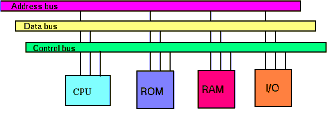
Fig 4_1: Computer System Block Diagram
The address bus is used by the processor to select a specific memory location within the memory subsystem, or a specific peripheral chip.
The data bus is used to transfer data between the processor and memory subsystem or peripheral devices.
The control bus provides timing signals to synchronise the flow of data between the processor and memory subsystem or peripheral devices.
![]() The
Central Processor
The
Central Processor
The central processor (CPU) is the chip which acts as a control
centre for all operations. It executes instructions (a program)
which are contained in the memory section.
Basic operations involve
The CPU is said to be the brains of any computer system. It provides all the timing and control signals necessary to transfer data from one point to another in the system.
![]() Programlar:
Instructions and Operand's
Programlar:
Instructions and Operand's
A program consists of a number of CPU instructions. Each
instruction consists of
The instruction code specifies to the CPU what to do, where the data is located, and where the output data (if any) will be put.
Instructions are held in the memory section of the computer system. Instructions are transferred one at a time into the CPU, where they are decoded then executed. Instructions follow each other in successive memory locations.
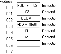
Fig 4_2: Program Instructions
Memory locations are numbered sequentially. The processor unit keeps track of the instruction it is executing by using a internal counter. This counter holds the location in memory of the instruction it is executing. Its name is the program counter (sometimes called instruction pointer).
![]() Stored
Program Control
Stored
Program Control
Most computer systems today are stored program control systems.
This means that the processor executes instructions which are
stored in a memory subsystem. SPC systems are popular, because
the processor does is simply changed by altering the instruction
in the memory system. This makes for a general purpose computer
system, capable of performing a wide variety of different tasks
dependant upon the stored program contents.
![]() Computer
Memory
Computer
Memory
Memory contains data or instructions for the processor to
execute. All memory has common features.
Each memory location is referred to as an address, and generally expressed in hexadecimal notation (using base 16 numbers).
The processor selects a specific address in memory by placing the address on a special multi-bit bus called the address bus . The value on this address bus is used by the memory system to find the specific location within the chip which the processor is requiring access to.
The total number of address locations which can be accessed by the processor is known as its physical address space. How large this is determined by the size of the address bus, and is often expressed in terms of Kilobytes (x1024) or Megabytes.
![]() Types
of Computer Memory
Types
of Computer Memory
System memory consists of two main types.
ROM is non-volatile. This means the contents do not disappear when the power to the system is turned off.
EPROM is a special type of ROM which can be programmed by the user. Its contents can also be erased by exposing it to ultra-violet light.
EEPROM is another special type of ROM which can be programmed by the user. It contents are erased by applying a specific voltage to one of its input pins whilst providing the appropriate timing signals.
| Advantages | Disadvantages | |
| Dynamic RAM | Cheaper Low Power High Density |
Slower Needs refreshing |
| Static RAM | Faster No need to refresh |
More Expensive Consumes More Power Low Density |
![]() Cache
Memory
Cache
Memory
Cache memory is high speed memory which interfaces between
the processor and the system memory. Dynamic memory is used to
implement large memory systems in modern computers. This is due
to features like low power consumption, high chip densities and
low cost.
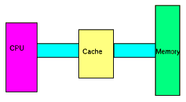
Fig 4_3: Cache Memory
Dynamic memory is however slow, and cannot keep up with modern fast processors. When a processor requests data from a memory chip, it expects to receive that data within a specific time. This is expressed as a number of clock cycles.
It is common for processors to run what is called a FOUR STAGE BUS CYCLE (which is four processor clocks long). Essentially, during the first processor clock cycle, the address is placed on the address bus. the second processor clock cycle is used to latch the address internally within the memory chip. The third processor clock cycle is used by the chip to find the data and place it on the data bus. The fourth processor clock cycle is used by the processor to latch the data on the data bus into its own internal hold register.
Dynamic memory is currently too slow to keep up with processors running at clock rates of 50MHz or greater (each cycle is 20ns). To use dynamic memory with fast processors requires extending the third processor clock cycle by another (or multiples thereof) processor clock cycle. The name for this extra processor clock cycle is called a wait state. What this does is change a four stage bus cycle into a five stage bus cycle (or greater), meaning that the fast processor is actually running just as fast as a slower processor (its being slowed down by the memory subsystem, whenever it accesses memory).
It is too expensive to use static memory in place of dynamic memory. To use slow dynamic memory with a fast processor requires an extra hardware subsystem (called cache memory) which fits between the processor and the memory subsystem.
All memory accesses by the processor are fed through the cache system. It comprises an address comparator which monitors the address requests by the processor, high speed static ram, and extra hardware chips.
The cache system starts off by trying to read as much data as possible from the dynamic memory subsystem. It stores this data in its own high speed static memory (or cache). When a processor request arrives, it checks to see if the address request is the same as that which it has already read from the memory sub-system. If it is, it supplies the data directly from its static cache. If the address is not cached, then it lets the processor access the main memory system directly (but the processor does this slower). The cache system then updates its own address counter it uses to read from system memory to that of the processors, and tries to read as much data as possible before the next processor request arrives.
When the cache system can respond to the processor request, its called a cache hit. If the cache system cannot service the processor request, its called a cache miss.
![]() Input/Output
Bus
Input/Output
Bus
The IO bus is the interconnection path between the processor and
input/output devices (including memory). The bus is divided into
THREE main sections
In more complex systems, the memory subsystem or peripheral devices also provide timing signals to complete data transfers, or initiate requests that the processor responds to (called interrupts).
![]() Input/Output
Peripheral Devices
Input/Output
Peripheral Devices
Peripheral devices allow input and output to occur. Examples of
peripheral devices are
The processor is involved in the initialisation and servicing of these peripheral devices.
![]() Input/Output
Processors
Input/Output
Processors
An input output processor is a special processor dedicated to
handling peripheral devices like terminals, tape and disk units,
and printers.
Mainframe systems like the IBM 370 use I/O processors to off load work from the system processor. This lets the system processor get more work done executing user programs without having to worry about handling data input and output to terminals or printing documents.
The PC has an I/O processor in the keyboard, which handles the complex operations of scanning the keys.
In addition, it is now becoming common to have I/O processors on graphics cards. The S3 graphics card is a good example of this, which supports hardware support for scrolling, sizing and moving windows. This removes these tasks from the system processor, and performs them at a much higher rate (up to 30 times faster).
![]()
![]()
Home | Other Courses
|
Notes
|
Tests | Videos
© Copyright Brian Brown, 1992-2001. All rights reserved.