![]()
Temel donanım bilgileri
© Copyright Brian Brown, 1992-2001. All rights reserved.
![]()
![]()
CPU AND MEMORY, Part 2
![]() IO
CHANNEL COPROCESSOR (IBM)
IO
CHANNEL COPROCESSOR (IBM)
To allow concurrent operation of the CPU and I/O devices requires
the use of a special I/O processor. The main CPU instructs the
I/O processor to perform the required data transfer. When the
transfer is completed, the I/O processor informs the main
processor of the status of the operation.
This method frees the main processor to perform other tasks whilst I/O is being done (tasks requesting I/O are blocked by the OS and thus not scheduled for processor time).
Typical features of an I/O channel processor system are
There are two main types of IO channels
Both channels support a number of devices on a bus called a sub-channel.
The selector channel operates in burst mode only. It handles a single sub-channel at a time, and has very high transfer rates. Typically, it controls high speed disk units.
The multiplexor channel handles more than one sub-channel at a time by interleaving requests. It operates in byte and word mode, but does support burst at a much lower rate than a selector channel. Typically, it handles devices like printers and character terminals.
Channel Operation
The processor initiates an I/O transfer by setting up a special
IOC program in main memory. It then issues a STARTIO instruction,
which identifies the channel and sub-channel.
The channel then accesses and runs the channel program (the address of which is in location 72). When finished, the channel updates the IO flag in the processors status register to signal command completion. The processor then checks the channel status register for results.
Each channel gets informed of
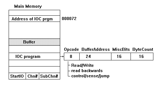
Fig 4_4: IBM Channel Operation
![]() The
Central Processor Revisited
The
Central Processor Revisited
We shall now take a closer look at how the processor functions
internally.
The Fetch, Decode, Execute Cycle
Most modern processors work on the fetch, decode, execute
principle. This is also called the Von Nuemen Architecture.
The execution of an instruction by a processor is split into
THREE distinct phases, Fetch, Decode, and Execute.
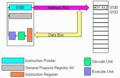
Fig 4_5: Fetch Cycle, reading the instruction
In the above image, the processor is ready to begin the Fetch cycle. The current contents of the instruction counter is address 0100. This value is placed on the address bus, and a READ signal is activated on the control bus. The memory receives this and finds the contents of the memory location 0100, which happens to be the instruction MOV AX, 0.
The memory places the instruction on the Data Bus, and the processor then copies the instruction from the Data Bus to the Instruction Register.

Fig 4_6: Decode cycle, decoding the instruction
In the above image, the processor transfers the instruction from the instruction register to the Decode Unit. It compares the instruction to an internal table, and when a match is found, the table contains the list of macro instructions (a number of steps) which are required to perform the instruction. In our case, the instruction means place the value 0 into the AX register. The decode unit now has all the details of how to do this.
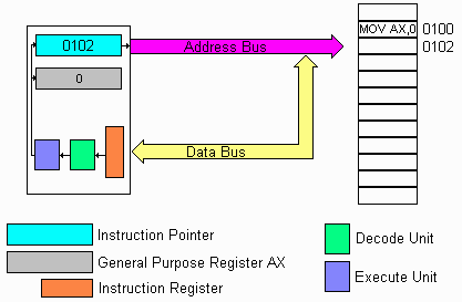
Fig 4_7: Execute cycle, executing the instruction
In the above image, the processor executes the series of macro instructions related to the instruction MOV AX,0. The final part is to adjust the Instruction Counter to point to the next instruction to be executed, which is found at address 0102.
Graphical Animation of
Instruction Fetch
The following graphic animation illustrates typical operation of
an instruction by the processor. It places the contents of the
instruction pointer onto the address bus and fetches the
instruction. Once decoded, the instruction is executed and the
instruction pointer altered to point to the next instruction.
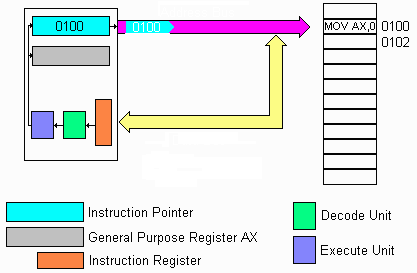
Fig 4_8: Animation of Instruction Fetch
We shall now look at the internal operation of the CPU, and how it performs the fetch, decode, execute cycle. Internally, the CPU is made up of a number of discrete sections.
The ALU normally works on two numbers at a time. Often,
one of the numbers is found in an internal location of
the processor, whilst the other is a constant or found in
the memory system. The reason for most arithmetic and
logic operations using operand's which are located inside
the processor is speed. This is due to not having
to perform a fetch cycle for transferring the operand
from the memory system to an internal hold point (called latch)
in order to execute the instruction.
The purpose of the ALU is to perform arithmetic and logic operations .
During the fetch cycle, the processor places the contents of this counter on the address bus. A read signal is issued on the control bus, then timing signals are generated to transfer (copy) the instruction from the memory location in system memory to an internal hold latch inside the processor (called the instruction register).
During the decode cycle, the instruction counter is adjusted to point to the next instruction to be executed from system memory (calculated from the current instruction).
The purpose of the instruction pointer is to hold the address of the instruction the processor is about to execute from system memory.
The decoded instruction might look like
The purpose of the instruction register is to hold a copy of the instruction which the processor is about to execute.
The reason why internal register banks (a group of registers) are used is speed. Data inside the processor is manipulated significantly faster than data external to the processor (ie, located in system memory). This is because of the time required to fetch the data from system memory and transfer it into an internal hold latch before it can be manipulated.
For instance, to multiply the contents of a memory location by 2, the processor needs to first read the memory location value to an internal register, transfer it to the accumulator, multiply it by 2, then write the ALU contents back to the memory location. The two memory cycles consume time.
In contrast, to multiply an internal register by 2 requires no external system memory access, and the lack of this overhead means that instructions of this type execute faster than those which make external references to system memory.
The purpose of internal processor register banks is to provide temporary storage for variables and calculations.
![]() The
Programming Model of a CPU
The
Programming Model of a CPU
The programming model of a processor defines the registers within
the processor which are visible and programmable by the user.
These include
Executing a program: An example
Lets consider the operation of the following program at the
processor level.
	Assembler	High Level Language
	MOV AX, #1 	A := 1;
	MOV BX, #2 	B := 2;
	ADD AX, BX 	C := A + B;
	PUSH AX 	Writeln( C );
	CALL WRITELN
Assume that the instruction pointer contains the address of the first instruction.
![]() Base
Units
Base
Units
The computer base unit houses the CPU, memory, floppy disk, hard
disk drive, power supply unit, and peripheral cards which support
printers and modems.
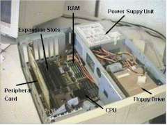
Fig 4_9: Computer Base Unit
The expansion slots are used to plug in additional peripheral cards like sound cards, TV Tuners cards, video capture cards etc. The two main types of expansion slots are PCI and ISA.
![]() Summary
Summary
Most modern Processors work on three cycles, fetch, decode and
execute.
Processors use internal temporary storage areas for holding data, these are referred to as registers.
The set of registers which programmers can alter is referred to as the programming model.
The Arithmetic Logic Unit handles mathematical operations like add, subtract, multiply, divide, shift and rotate.
![]()
![]()
Home
|
Other Courses
|
Notes
|
Tests
|
Videos
© Copyright Brian Brown, 1992-2001. All rights reserved.