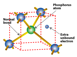
You have to remember that up until this point, both sides of the silicon are electrically neutral. The n-type silicon with extra electrons is offset by the extra protons in phosphorus. The p-type silicon which is missing electrons is also missing protons because of the boron.
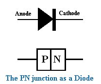
When these two sides come together, there is a mad race for the electrons on the n side to find a place on the p side. If all of these extra electrons found a place, then this would be of no use because the entire piece would be neutral. The key is that not all of the extra electrons find a place on the p side. Many of the electrons in the n-type silicon line up on the edge of the barrier between the n-type and p-type silicon, and this creates an electric field between the two sides. This line up of electrons on the edge of the silicon is called a diode. It allows electrons to easily go from the p-side to the n-side, but not the other way around. This means we have a flow of electrons that can only go in one direction, which is required for electricity.