| Methods
for determining properties of Semiconductors
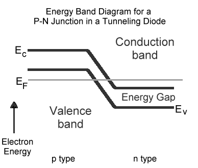
1. The minimum energy gap
|
Semiconductors are physically available as Group
IV elements and their associated compounds. The most common semiconductor
materials are the elements Silicon and Germanium. Semiconductors in general
have similar properties but posses particular traits that enable us to
differentiate them.
In this section, we will discuss the various methods of determining the characteristic properties of semiconductors. 1. The minimum energy
gap DE
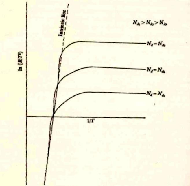
The simplest method, in principle, for obtaining the value of DE is to observe the variation of the intrinsic conductivity i with temperature. i = ni(b+I)uh Also, the intrinsic carrier concentration ni, for non-degenerate condition, is given by the equation ni = AT^3/2exp(-DE/2kT), where A is a constant whose value depends on the effective masses of holes and electrons. All these values can then be used to plot a graph of RT^3/2 against I/T. For an element semiconductors such as Ge and Si good straight lines are obtained for such plots but this is not so for all semiconductor. At sufficiently high temperatures the curves of all specimens tend to
a curve known as the 'intrinsic line' and this is taken to the variation
of the intrinsic Hall constant.
2. Mobility of electrons
and holes
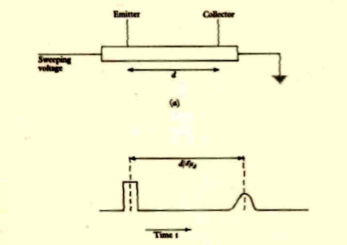
The most direct method of measuring the drift mobility ud of electrons and holes is that derived from the drift experiment of J.R Haynes and W. Shockley. The method consists essentially of injection of a narrow pulse of minority carriers into a filament and sweeping the pulse along the filament by means of an electric field. The passage of the pulse past the collector contact is observed by means of a cathode-ray oscilloscope. When the positive voltage-pulse producing an electric field E is applied to the emitting contact, a similar pulse apperars almost at once at the collector contact, the time delay corresponding to the propagation time of an electromagnetic pulse down the filament at a later time of the order of l/Eud, where l is the distance between the emitter and collector contacts, the pulse of minority carriers arrives between the collector contact and gives rise to a voltage pulse at the output, since the holes change the collector current. For example, for n-type Ge, udh = 1900 cm^2/Vsec.
so that if E = 10V/cm, which is a typical value for such an experiment,
we have t = 30usec.
3. Carrier concentration
If the mobility ratio b is known, the intrinsic carrier concentration ni may be obtained, with the same uncertaintainty as regards r, from the intrinsic Hall coefficient. If r is known from drift mobility measurements from ni may be obtained precisely by this method; only for Si and Ge is this possible, at the moment. If the band structure and values of the various effective masses are known, such as for Si and Ge, ni may be calculated for any value of the temperature. When the effective masses are not known, only an order of magnitude may be obtained for ni when the forbidden energy gap is known, by using free electron mass m. For semiconductors such as InSb, in which b is very large, ni may be deducted from the conductivity of intrinsic samples if un is known, the contribution of the holes to the conductivity being extremely small. Values of ni for Si and Ge are known with considerable accuracy over a wide range of temperatures. For InSb and InAs, accurate values have also been obtained; for PbS, PbSe, PbTe the values are known with somewhat less accuracy. At the moment these are the only semiconductors for which ni is known
except as to the order of magnitude.
4. Thermal Method
Under these conditions, the creation of hole-electron pairs due to thermal excitation from the valence band to the conduction band is usually negligible. The carrier concentration is determined by measurement of the Hall constant
at low tempratures.
5. Minority carrier lifetime
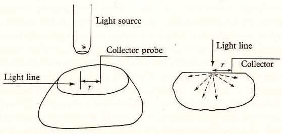
A variation of this method, useful for testing bulk samples of Si and Ge has been described by F.S. Goucher. This consists of injecting carriers by means of a fine line of light on the plane face of a sample, and measuring the variation in the collector current from a point contact as a function of distance from the line of light. One refinement for this method is to take account of the cylindrical symmetry of the excess carrier concentration, which falls off exponentially with distance from the light line. The above method has been applied extensively to determine lifetimes in Si and Ge. Serious difficulties however have been encountered in its use with Si. With Si, the departure from linearity of the collector charactristic
can be very marked, but this can be overcome by illuminating the collector
point with steady light and varying the light used forinjection, scattering
the light used for injection into the region of the crystal near the collector
point can lead to serious errors.
|
Germanium is one of the common semiconductor materials.
|