
PCB
A PCB (printed circuit board) holds components together & provides electrical conductivity in between them.
Guidelines:
1 / 6. prepare artwork
Draft out schematic preferably with a PCB program, and print out the circuit layout onto clean transparent film. Otherwise, create the circuit layout by rubbing down dry transfers on transparent film. The artwork must be sharp & opaque.
2 / 6. expose PCB with artwork
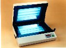
Remove protective film on PCB to reveal photo resist side. Lay artwork on photo resist side of PCB, & place them in UV exposure unit, facing the UV tubes. Close lid and set timer. Usually 60-90 seconds is enough.
3 / 6. develop exposed PCB
Submerge exposed PCB in developing solution and agitate it to wash off exposed photo resist. Dark circuit layout lines should appear distinguish from the copper. If layout lines are broken, small breaks can be mended by applying oil-based dark marker pen.
4 / 6. etching developed PCB
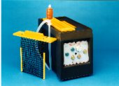
Submerged PCB into Ferric Chloride solution for etching. It should be done around 15-30 min. The circuit should appear clearly. Be reminded that this solution is corrosive.
5 / 6. wash
Spray wash PCB. Scrub clean from any impurities. Tin plating solution (powder dissolved in water) may be used to make a bright, highly solder-able finish on the copper tracks.
6 / 6. drillings
Drill respective holes on PCB for components placements. Drill holes at corners for spacers so that board can be fastened to chassis.
The completed amplifier circuit is now ready for use.
![]() PCB
PCB