-
Introduction
The remarkable
characteristic of transistors that fuels the rapid growth
of the information technology industry is that their speed
increases and their cost decreases as their size is reduced.
The only other product in manufacturing with this characteristic
over such a vast range of size reduction is the hard disk
drive with magnetic storage. The transistors manufactured
today are 20 times faster and occupy less than 1% of the area
of those built 20 years ago. It seems intuitively obvious
that continued reduction of the area of a transistor by a
factor of 2 every three years cannot be sustained forever.
However, predictions of the limit of size reduction or even
of the pace of size reduction have proven to elude the most
insightful prognosticators. The predicted limit has been
dropping at nearly the same rate as the size of the transistors.
The accuracy of a prediction of the future of CMOS technology
is therefore not likely to be very great. However, the key
principles underlying the evolution of CMOS technology can
give us some insight into the future.
A recent
study by Taur et al. [1] pointed
out that the particular transistors in dominant use today
(complementary p-type and n-type field-effect transistors,
called CMOS) will soon have a lower rate of performance increase
as their size is reduced. Taur advocated a focus on exploratory
devices, low-temperature operation, and increased functional
integration as means of sustaining the industry trend of system
performance improvement [1].
This paper examines these and other, broader, issues related
to the future development of CMOS technology. It is concluded
that the current rate of transistor performance improvement
can be sustained for another 10 to 15 years, but only through
the development of new materials and transistor structures.
In addition, a major change in lithography will be required
to continue size reduction. Memory technology for DRAM products
is similarly reaching a major hurdle and requires a new architecture
to move beyond 1Gb levels.
The most
common description of the evolution of CMOS technology is
known as Moore's law. It is important to understand the key
principles underlying Moore's law, since these allow us to
gain insight into the future. The observation made by Gordon
Moore in 1965 was that the number of components on the most
complex integrated circuit chip would double each year for
the next 10 years [2]. This
doubling was based on a 5060-component chip produced
in 1965 compared with those produced in preceding years, starting
with the single planar transistor in 1959. In 1975 Moore noted
with amazement that his previous prediction had come true
[3]. He predicted, however,
that in the future the number of components per chip would
require nearly two years rather than one year to double. He
believed that this change in slope would occur in 1980, but
it happened earlier, in 1975. In the last 20 years this prediction
has been remarkably realized and has gained the status of
a law. The term Moore's law has come to refer to
the continued exponential improvement in the cost per function
that can be achieved on an integrated circuit.
The importance
of Moore's law lies not in the constancy of the rate of increase
but in the root cause and in the effect of the trend. Moore
pointed out in his original paper that the doubling of the
number of components on an integrated circuit was due to three
factors. First, and most significant, half of the increase
is derived from improvement in lithographic resolution. Second,
25% of the increase is due to larger chip sizes, made possible
by enhanced manufacturing techniques and better lithography.
Third, the remaining 25% is due to innovation, such as more
creative techniques for forming the components, predominantly
transistors, on a chip. These three factors are the driving
forces behind the trend for increasing the number of components
on a chip.
Moore
also pointed out that the result of this increase in components
per chip is a lower cost per component. The basic assumption,
of course, is that the increase in the cost of fabricating
a chip is less than the increase in the number of components.
The resulting dramatic exponential reduction in cost per function
is really the fuel behind the semiconductor industry and the
information technology age. The key is not the constancy of
the rate of increase known as Moore's law, but that the rate
of increase of components (and the corresponding function)
is greater than the rate of increase of the cost per chip.
The doubling rate of Moore's law has changed in the past and
may change again in the future, but as long as the cost per
function continues to decline, the information revolution
will continue unabated.
Performance
was not an explicit parameter addressed in Moore's original
paper. However, associated with the increase in the number
of transistors on a chip is the improvement in performance.
This is not an automatic consequence, but rather the result
of careful design. The increase in processor performance results
from both an increase in density and an improvement in transistor
design.
The key
to understanding the future of CMOS technology is to understand
the factors influencing the cost per function. CMOS will continue
to dominate and evolve as long as the net cost per function
drops. This paper therefore considers the key elements behind
this trend:
-
Lithography to enable the manufacturing of components with
smaller dimensions. As Moore pointed out, this is the single
greatest factor in increasing the number of components per
chip.
-
Proper transistor design to achieve higher performance at
smaller dimensions as well as innovative layout to gain
density.
-
More effective interconnections to increase the component
density.
-
New circuit families.
-
Innovative, denser memory cells.
-
More productive design processes.
-
Manageable capital costs.
Lithography
Lithography
is the means by which patterns are delineated on wafers and
is therefore the primary driving force behind the reduction
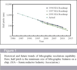
of the size of transistors. Figure 1
shows the historical and predicted trends of lithographic resolution
capability. Optical (approximately visible-wavelength light)
lithography was once thought to be limited to >1-µm resolution,
but the industry is now moving to 0.18-µm resolution in
manufacturing. One interesting point to note in Figure
1 is that recent progress in lithography has exceeded the
pace of most predictions.
 Figure
1 Figure
1
One way
to discuss lithography is in terms of linear dimensions, comparing
the smallest feature to be patterned with the wavelength of
the light used for the lithographic process. The first widely
used light sources in the industry were mercury lamps, leading
to a focus on the specific emission lines of mercury. All
of the features defined had dimensions greater than the wavelength.
In recent years, the so-called g-line and i-line, with wavelengths
of 435 nm and 365 nm, respectively, have become industry standards.
The 365-nm light source has been used to pattern features
as small as 0.35 µm, essentially equal to the wavelength.
Below half-micron dimensions, a transition to deep ultraviolet
(DUV) light sources (either mercury source or, increasingly,
excimer lasers) at 248-nm wavelength has enabled lithographers
to pattern 0.25-µm dimensions, also equivalent to the
wavelength. The industry is now moving to 0.18-µm lithography,
marking the first time that features smaller than the wavelength
are being patterned. Future lithography will require patterning
features smaller than the wavelength and/or further reductions
in the wavelength, perhaps through the adoption of an entirely
new exposure source.
Patterning
features smaller than the wavelength of the exposure source
leads to significant challenges due to the diffraction of
light. Optical proximity correction techniques are therefore
a critical part of enabling future lithography. Various techniques
such as off-axis illumination and phase-shift masking enable
the patterning of features smaller than the wavelength. The
tradeoff requires more complex, costly masks and possible
design constraints. Potentially, it may be possible to define
features down to half the dimension of the wavelength. The
properties of the photoresist itself (the light-sensitive
exposed polymer) are also critical to the feature resolution
achievable.
Achieving
dimensions of 100 nm and below will therefore quite likely
require a reduction of the source wavelength. The industry
is actively engaged in preparing for a transition from 248
nm (with KrF excimer lasers) to 193 nm (with ArF excimer lasers).
Beyond that, there appears to be no industry consensus concerning
the next-generation lithography. The next possible small step
in wavelength could be at 157 nm (with F excimer lasers).
However, few materials are sufficiently transparent to be
used in refractive lenses or in masks. Calcium fluoride is
a leading candidate, but with its coefficient of thermal expansion
nearly 40 times that of quartz, it may be difficult to avoid
distortion. Special forms of quartz may be usable for masks,
but acceptable photoresist materials for this wavelength have
not yet been developed.
Several
non-optical lithography techniques are being explored in the
industry. Electron-beam lithography is capable of defining
extremely small feature size due to an effective wavelength
of the electrons of about 0.01 nm. E-beam lithography has
long been used for mask-making and for low-throughput wafer
exposures. However, the use of e-beam lithography for chip
fabrication will require greatly increased throughput. Schemes
for achieving sufficient throughput by using large-area electron
beams with blocking masks and electro-optic reduction lenses
are being explored. Two such efforts are PREVAIL [4]
and SCALPEL [5]. The key problems
to be solved are field stitching (multiple masks are needed
to cover a single chip), mask integrity, and cost. Proximity
X-ray lithography has been used by IBM to fabricate exploratory
integrated circuits at dimensions from 1 µm down to
0.15 µm. The 1.1-nm wavelength is extracted from synchrotron
radiation, such as that obtained from the Helios ring built
by Oxford Instruments and installed at the IBM technology
development facility in East Fishkill, New York. The primary
concern is that lenses and mirrors are not available for these
wavelengths. Blocking masks must be used with features of
the same dimension as that on the wafer. The cost and difficulty
of fabricating these masks without distortion are key challenges.
Other issues concern the close proximity (10 µm or less)
required between the mask and the wafer and the associated
diffraction effects. X-ray projection lithography, euphemistically
named EUV for extreme ultraviolet light, tries to avoid the
1× mask issue by using 1113-nm-wavelength light.
At that wavelength, it may be possible to construct reflective
lenses and reticles with a 4× dimension-reduction system.
However, the system requires concave lenses composed of a
superlattice of approximately 40 layers of 23-nm films,
with a local and global uniformity of atomic dimensions.
Other,
more exploratory approaches such as ion-beam lithography or
hot-electron emission lithography are being investigated.
At this time, however, none of these approaches has a high
probability of succeeding, and all would require major resource
investment to realize. The message is that lithography, the
major component of Moore's law, will face enormous challenges
in the coming years. Optical extensions will require radical
changes to shorter-wavelength light. Non-optical techniques
remain to be proven. The biggest risk is that the cost of
a new system might be greater than the derived benefit of
component density. Although exposure system costs might be
amortized over many products, high mask costs must be borne
by each product. Moore's law will continue to be effective
only as long as the cost per component continues to drop.
Transistor
scaling and design
History
From the time of its invention in 1948, the bipolar transistor
had been the choice for high-performance operation. The field-effect
transistor was demonstrated soon after the bipolar, but was
generally found to be a slower switching device. It was nonetheless
prominent in lower-power, higher-density circuit applications.
Both types of transistors exhibited the characteristics of higher
speed and lower power at smaller sizes. However, the power per
circuit could not be decreased as rapidly for bipolar transistors.
As linear dimensions reached the half-micron level in the early
1990s, the performance advantage of bipolar transistors was
outweighed by the significantly greater circuit density of CMOS
circuits using field-effect transistors. The system performance
benefit of integrated functionality superseded that of raw transistor
performance, and the dominant circuit in production today is
the CMOS circuit.
The evolution
of the basic transistor used in the CMOS circuit was predicted
with remarkable accuracy at the 1972 International Electron
Devices Meeting. Dennard et al. from the IBM Thomas J. Watson
Research Center presented a paper on the design of transistors
at very small dimensions [6].
They proposed a scaling theory which has guided transistor
design in the industry ever since. For any reduction  in linear dimensions, they showed how the voltage and the
doping levels could be tailored so that the performance would
increase by a factor of ,
the power decrease by a factor of 2,
and the power density remain constant. In 1974, Dennard et
al. published a device design for transistors with 1-µm
channel lengths, together with data on experimental transistors
[7]. However, such devices
were not used in manufacturing for another ten years or more.
in linear dimensions, they showed how the voltage and the
doping levels could be tailored so that the performance would
increase by a factor of ,
the power decrease by a factor of 2,
and the power density remain constant. In 1974, Dennard et
al. published a device design for transistors with 1-µm
channel lengths, together with data on experimental transistors
[7]. However, such devices
were not used in manufacturing for another ten years or more.
In practice,
threshold voltages cannot be scaled rigorously without lowering
the operating temperature, and the power density has increased
somewhat over time, but the basic scaling principles have
been largely followed. Threshold voltages were not reduced
according to scaling theory primarily because of consideration
of the off current. Perfect scaling would have reduced the
operating temperature of the transistor so that the off current
would remain constant. The practical consideration of keeping
the operating temperature at room temperature or above meant
a sacrifice of some off current and dictated a threshold voltage
of about 0.3 V or higher. The power-supply voltage was therefore
also kept higher than scaling theory dictated in order to
achieve performance at the expense of power density.
Inevitably,
the scaling process will soon reach the point at which no
further compromise of voltage levels can be made to achieve
higher performance without lowering temperature significantly.
Figure 2 shows the prediction
of a diminished rate of increase in performance for future
CMOS technologies.
 Figure
2 Figure
2
The potential
impact of this diminished rate of performance gain on microprocessor
clock frequency is shown in Figure
3. Clock frequency improvement is due partially to
transistor performance and partially to improved logic and
circuit design. The solid curve assumes that both trends will
continue at the current rates, leading to a prediction of
20-GHz processors in the year 2010. The lower bound indicates
the effect of no further logic and circuit design improvement
beyond 1 GHz and the transistor performance trend of Figure
2. The result would be a 1.5-GHz processor limit. The
most likely scenario is that new materials and devices as
well as further circuit design learning will lead to continued
improvement of clock frequency, but possibly at a slightly
slower rate, as shown in Figure 3.
Considering the growing opportunities for system enhancement
through software and I/O design, this rate should be sufficient
to sustain Moore's law.
 Figure
3 Figure
3
Scaling limits vs. fundamental limits
The limitations to the extendability of transistor scaling
theory are concerned primarily with tunneling through the
gate oxide and the ability to deal with short-channel effects.
That is, as the dimensions are reduced without a corresponding
reduction in temperature to lower the off current, the power-supply
voltage, the threshold voltage, and the doping profile must
be adjusted to maintain a useful ratio of on current to off
current. At some point, tunneling through the gate oxide and
other effects limit the achievable channel length so that
no further performance can be achieved.
The gate-oxide
tunneling effect is therefore a major factor limiting transistor
scaling. The limit is approximately 11.5 nm compared
to the 3.5 nm in production today. These oxides would be only
five or six atomic layers thick. Recent results [8]
also indicate that these tunneling currents can initiate damage,
leading to previously unexpected reliability concerns in very
thin gate dielectrics. Reliability concerns might limit gate-oxide
thickness to 1.52.0 nm. New device structures or a new
gate oxide with a higher dielectric constant will have to
be developed to enhance performance without further reduction
of the gate-oxide thickness. No scaling theory exists to guide
either development. In this sense, we will indeed soon reach
the limits of CMOS scaling.
Fundamental
limits such as thermal motion of carriers in a solid or the
uncertainty principle are shown by Meindl [9]
to be far beyond practical considerations of devices. Of more
practical interest are limitations of novel device structures.
Independent of the specific structure, the limit of a useful
device with an on/off current ratio of 1000 due to sourcedrain
tunneling alone appears to be about 5 nm separation of the
source and drain. Accounting for dopant fluctuations and screening
effects, an ultimate lower limit may be assumed to be 10 nm.
Meindl estimates a more conservative limit of the order of
25 nm. In either case, at most another factor of 10 in linear
scaling (about 15 years at current rates) can be anticipated
before ultimate limits are reached. The technical challenges
of scaling CMOS to below the 0.1-µm level have been
articulated in more detail elsewhere in the IBM Journal
of Research and Development [10].
Novel transistor structures
Without a change in transistor structure, scaling at room
temperature will lead to a reduction in the performance improvement
rate in a few years. The difficulty in changing structures
should not be minimized. Historically, the switch from metal
gates to polysilicon gates, the switch from diffusion to ion
implantation, and the incorporation of silicides were major
changes that were difficult to implement, even though the
transistor structure itself was little changed. A novel device
structure will be even more difficult to produce.
Two types
of structure and materials changes must be considered. First,
there are structures that allow a shorter channel length to
be fabricated. Second, there are materials that enable higher
performance for a given channel length.
Figure
4 shows a set of exploratory transistor structures
that enable scaling to shorter channel lengths. The first
variation from the standard bulk device is a silicon-on-insulator
(SOI) device. This structure has been studied for decades
in the industry, but only recently has the defect density
resulting from implantation damage or other methods of insulator
formation been reduced sufficiently to make it feasible. IBM
has considerable experience with these devices, and a performance
gain of 2030% could be realized. In addition, transistors
could be scaled to smaller dimensions with SOI, but possibly
only one step beyond traditional devices.
 Figure
4 Figure
4
The next
two device structures include a ground plane or some kind
of conductive layer underneath the device channel to act as
an electrostatic mirror, providing a higher-performance
channel. These are variations on the path to the ultimate
double-gate device pictured at the bottom of Figure
4. This ultimate structure effectively has two channels
(one for each gatesilicon interface) to double the current
capacity and a symmetrical design that helps minimize short-channel
effects. Unfortunately, it is too early to know whether these
devices are actually manufacturable. Simulation, supported
by measurements on experimental hardware, indicates that if
they can be built in the next 15 years, their performance
will likely maintain the performance improvement pace of the
1990s (Figure 5).
 Figure
5 Figure
5
Another
class of devices depends on material modifications to enhance
mobility and therefore the performance at a given channel
length. For example, SiGe deposition could be used judiciously
to form strained Si layers or SiGe layers that could enhance
the mobility of either electrons or holes. Enhancing both
electron and hole mobilities at the same time requires a rather
complex set of layers. Performance enhancement may range from
30% to 60%, depending on usable mobility factors. It is not
yet clear whether these materials can be combined with the
short-channel structures described above.
Low-temperature operation
In principle, the inability to reduce the operating temperature
commensurately with the other variables limits the scaling
potential of transistors. It seems obvious, therefore, that
a reduction in operating temperature could improve performance.
This effect has been thoroughly studied in the industry, led
by IBM. It is clear that performance improvements up to a
factor of 2 can be achieved if the temperature is lowered
to liquid nitrogen temperature (195°C). However,
practical considerations of refrigerator cost and reliability,
as well as the need to redesign the technology for optimized
low-temperature operation, have inhibited commercial realization
of low-temperature operation. Historically, the prospect for
continued scaling at room-temperature operation always offered
the possibility of a more traditional answer to improved performance.
Now, with the greater difficulty in scaling devices and with
improvements in refrigerators and in the silicon technology
itself, low-temperature operation may be commercially feasible,
at least for high-end servers. Optimum cost/performance operation
may be at 50°C, where refrigerators can perform fairly
efficiently and little modification of the silicon technology
is required. A performance enhancement of approximately 50%
is anticipated at this temperature. In the longer term, an
opportunity exists to exploit the 2× system performance
at liquid nitrogen temperature by developing the necessary
low-threshold CMOS, packages, and cryocoolers.
Although
high-end servers are considered to be the best candidate for
effective use at low temperatures, the high power consumption
of these systems also requires fairly high-capacity refrigerators.
Thermoelectric materials offer a low-cost, solid-state method
for cooling chips, though at temperature differentials of
only a few tens of degrees and power levels of tens of watts
at most. Nevertheless, some performance enhancement may be
possible. Providing additional cooling when portable systems
are docked can also increase performance. These possibilities
warrant further research.
All of
the exploratory devices mentioned above offer higher performance
at low temperature, though the magnitude of the effect may
vary depending on the specific device. Significant improvement
in the resistivity and capacitance of interconnections will
also enhance performance. Potential performance vs. time for
low-temperature operation of these devices is shown in Figure
5.
Wiring
and interconnections
The wiring
required to interconnect transistors must scale at the same
rate as the transistors in order to take advantage of improvements
in size and speed. The industry is currently moving from aluminum
to lower-resistance copper metallurgy, which can decrease both
wiring resistance and capacitance. Research is also underway
to move from silicon dioxide insulators between wiring levels
to various low-dielectric-constant insulators, which can further
decrease wiring capacitance. Despite these major changes in
materials, there is a concern that owing to higher resistivity
and capacitance, the extremely small wires will be unable to
support performance enhancements. Here, the solution appears
to be a hierarchical wiring scheme, which combines high-density
wiring capability at the first few levels with larger, lower-resistance
and -capacitance wiring at the upper levels. This hierarchy
simultaneously meets the need for density and performance. With
this approach, wiring density will in fact be able to support
whatever density can be achieved with the lithography and transistor
designs discussed above. An in-depth discussion of the future
of interconnections is found in a companion paper in this issue
[11].
Circuit
families
The rise
of CMOS technology is a classic study of the power of integration
through high density. So far, we have discussed the role of
lithography, transistor design, and interconnections as means
of putting more components on a chip, in order to achieve our
economic goal of reducing cost per function. However, power
dissipation concerns have played a key role in establishing
CMOS as the predominant circuit family in the semiconductor
industry.
Field-effect
transistors (FETs) evolved from p-type metal-oxide-semiconductor
FETs (p-MOS) in the 1960s to n-type MOS (n-MOS) in the 1970s
and then to CMOS in the 1980s and 1990s. The p-type FETs were
first used by many in the industry because of their lower
sensitivity to mobile ion contaminants such as sodium. However,
n-type FETs are significantly faster because electron mobility
is much greater than hole mobility. The industry soon learned
to develop effective clean rooms and contamination control,
enabling the move to n-MOS circuits. Enhancement and depletion-mode
devices were used to fabricate efficient circuits. CMOS circuits
combine both n-MOS and p-MOS in a way that greatly reduces
power consumption. The main disadvantages of CMOS were the
added process complexity, somewhat lower performance, and
the tendency for latch-up to occur. Latch-up, or locking of
the circuit in a high-current mode, was due to parasitic transistor
action. The advantages of CMOS were added logic capability
and lower power dissipation. Ultimately, the lower power dissipation
allowed more components to be utilized in an integrated circuit
than with n-MOS. The processing challenges were resolved,
latch-up was avoided with modern circuit design, and CMOS
became the dominant circuit family. It was clearly a case
of density winning over performance, with the slower-performing
circuit family improving sufficiently rapidly in density to
mitigate its handicap.
While
the FET market was evolving for cost performance applications,
the high-performance portion of the semiconductor business
was dominated by bipolar transistor designs. Since these bipolar
transistors had a vertical structure rather than the horizontal
layout of the FETs, the active region of the device was much
smaller. Furthermore, with current-mode operation rather than
field-effect operation, the overall performance of the bipolar
was significantly higher than that of the FET. The current
drive capability was much greater, and there seemed to be
no contest between CMOS and FET when premium performance was
required. However, by the early 1990s, it was becoming clear
that a large number of components on a chip could lead to
superior system performance as well as lower cost per component.
At high integration levels, functions that otherwise required
many chips and complex system connections could be combined
onto one chip. The net effect was improved chip performance
as well as a significant reduction in cost. Despite the raw
transistor speed advantage, bipolar circuits had much greater
power dissipation, and hence lower density, than CMOS circuits.
Eventually, CMOS technology was able to achieve greater system-level
performance, thanks to high integration levels, despite its
inherently slower transistors.
This transition
is dramatically illustrated in Figure
6 and Table 1 for the
IBM S/390 systems. The G6 system, first shipped in 1999, offers
more than double the performance of the fastest bipolar system
shipped, and yet it contains dramatically fewer components
and has much lower space and power requirements.
 Figure
6 Figure
6
| Table
1 Comparison of physical characteristics
of bipolar and CMOS-based IBM S/390 systems. |
|
|
ES/9000*
9X2 |
S/390*
G6 |
|
| Technology |
Bipolar |
CMOS |
| Total
no. of chips |
5000 |
31 |
| Total
no. of parts |
6659 |
92 |
| Weight
(lb) |
31,145 |
2057 |
| Power
requirement (kVA) |
153 |
5.5 |
| Chips
per processor |
390 |
1 |
| Maximum
memory (GB) |
10 |
32 |
| Space
(sq ft) |
671.6 |
51.9 |
|
What will
happen to CMOS circuits in the future? Will CMOS itself eventually
be replaced by another circuit family providing another dramatic
shift? At present, it does not appear that there is a viable
contender to displace CMOS. FET products were on the market
for decades in lower-cost, lower-function products before
finally maturing to the point of displacing bipolars in premium-performance
applications. However, no alternative logic technology is
evolving within cost/performance products on the market today
to threaten CMOS dominance. And in light of the continuing
CMOS performance evolution, an even steeper evolution and
learning curve would be necessary to displace CMOS. There
will likely be variations on CMOS circuits, but no radical
shift in circuit type seems to be on the horizon.
New alternative
technologies to silicon and CMOS are often proposed and explored.
Many of them utilize silicon technology as a base. In general,
most of these alternatives carry out a different function
than CMOS circuits and are more likely to succeed in special-niche
applications. For general-purpose computing and data handling,
CMOS technology appears likely to dominate for the foreseeable
future.
Memory
cells
Memory is
a critical part of a CMOS system; its size and performance must
be scaled in concert with the logic processor. In addition to
utilizing CMOS logic, a DRAM chip depends on a cell consisting
of a single transistor and a capacitor. Economic viability of
the DRAM industry has followed Moore's law more closely than
any other product. For twenty years, DRAM products have followed
a generational evolution leading to a 4× increase in bits
per chip every three years. As Moore predicted, half of this
was due to lithography resolution, a quarter to larger chip
sizes, and the rest due to cell innovation. We have discussed
lithography in a previous section and comment briefly on chip
sizes in the section on cost. Cell innovation deserves a closer
look.
Up through
the 1Mb DRAM generation, one-device cells in DRAM products
were planar cells. The transistor and capacitor were laid
out in a conventional fashion side by side to form the memory
cell. The innovative designs that reduced the cell size independently
of lithography came from process techniques such as self-alignment
or creative layout. For the 4Mb generation, IBM invented the
substrate plate trench cell, forming the capacitor vertically
in the substrate rather than horizontally. Others in the industry
chose a stacked-capacitor design, also forming the capacitor
vertically but placing it above the silicon substrate. Both
approaches continue to persist in the industry. The innovative
part of Moore's law is achieved by moving the capacitor and
transistor closer and closer on top of each other.
Conventional
design methodologies constrain the size limit of these cells
at eight times the square of the lithography dimension, a
limit which will be reached in the 1Gb DRAM product generation.
New architectural approaches to minimize noise may enable
the industry to go to six or even four times the lithographic
feature. However, the four-square cell marks the limit of
a cross-point cell. That is, if a memory cell location is
defined by the intersection of two orthogonal lines of minimum
dimensions and if this cell is separated from neighboring
cells by the minimum dimension, the area of the cell is four
times the square of the minimum dimension. It is challenging
indeed to form a transistor with its source, drain, and gate
and a capacitor within that area. Moving beyond that level
will require circuits that store and retrieve multiple bits
per cell, an unlikely development since the reduced signal-to-noise
ratio would likely offset any area advantage.
Memory
cells can therefore continue to scale according to Moore's
law, as long as lithography continues to scale, until the
four-square limit is reached. At that point (or sooner if
innovation fails to take us beyond six square cells), the
reduction in cell size will be due solely to lithography improvement.
If lithography also slows down, the memory progression will
taper off.
DRAM economics
may impose a different scenario. Moore's law really states
that the cost per bit must continue to drop in order for the
trend to continue. If lithographic techniques or process complexity
becomes more expensive than justified by the resultant bit-density
increases, further capacity improvement in DRAMs may not meet
the economic test. Alternatively, if volume demand fails to
materialize for a given generation, it may not be possible
to amortize the development and manufacturing costs over a
sufficient number of products. Such dire economic failure
has been predicted for many DRAM generations, but has never
yet occurred. As long as applications evolve to use gigabytes
of memory in high-volume information appliances, it may never
occur.
Design
Moore's law
focuses on the number of components on a chip. In his first
paper, Moore did not envision that one day there would be chips
with a billion transistors sold for less than $100. Now such
an event is likely in a couple of years. Yet, the function carried
out by these transistors depends on the design of the chip,
that is, the logical patterns in which the transistors are connected.
With such a vast number of components, the possibilities for
design variations are nearly infinite. Each transistor can have
a different length and width and threshold voltage. Each one
can be connected to almost any other transistor. The possible
number of combinations is unfathomable. The art of design is
to select that combination which carries out a specific function.
The complexity of function that can be achieved is now so enormous
that design automation and design verification have become factors
as important in CMOS technology evolution as the process technology.
Whereas
Moore's law emphasized the number of transistors on a chip,
the current relevant parameter is really the function that
is executed by those transistors. With such a vast number
of transistors, superior design techniques can elicit more
function on a chip without increasing the number of transistors.
Moore's law must therefore be transformed into a trend of
increased function rather than increased number of transistors.
As noted above, the number of transistors on a chip may not
have to increase as rapidly as it has historically in order
to sustain a similar rate of increase in function. The slope
of Moore's law has changed before, and it will likely change
again without major impact. A future reduction in the slope
of these trend lines will probably have little impact on the
industry trends because of the tremendous opportunity still
available for creative design, adding more function per number
of transistors on a chip.
In one
area of design, there appears to be a counter to Moore's law.
Modern microprocessors not only fit on one chip but actually
occupy only a small portion of a chip. The remainder of the
chip is usually devoted to cache memory and represents a tradeoff
of higher cost for higher performance. The shrinking size
of the processor is due to a greater increase in transistors
per unit area than in the number of transistors required for
a processor. With increasing clock rates, the allowable space
for a synchronized processor is shrinking faster than the
processor size. Processor clock rates will soon be in the
gigahertz range. For a 10-GHz processor, which we may reach
by 2010, the clock cycle time is 100 ps. Since light travels
at 300 µm/ps in vacuum, the space reachable by light
in one clock cycle is 30 mm. Assuming a medium consisting
of typical dielectrics rather than vacuum, the reachable space
is of the order of 1520 mm, roughly the size of today's
chips. Fundamental laws of physics tell us that information
cannot be conveyed over larger areas than that reachable by
the speed of light. Practical limitations may reduce this
range further. Fortunately, hierarchical design strategies
allow high-frequency portions to be localized in a small region,
and longer-range information transfer can be done at longer
clock cycles. However, this restriction on size is a fascinating
challenge to the trend toward increased chip size noted by
Gordon Moore.
Cost
Cost reduction
is a major tenet of Moore's law. The primary factor underlying
the decreasing cost per circuit or memory bit is the increase
in density, or circuits per square millimeter. The cost of processing
a silicon wafer must increase much less rapidly than the density
in order to achieve cost reduction. The rapid (25% per year)
increase during the 1980s of the capital cost of a silicon manufacturing
line led to concerns of diminishing returns in cost per circuit.
However, since 1990 the rate of increase has slowed to less
than 15% a year. Major factors behind this reduction were a
stabilization of clean-room requirements, better equipment productivity
and utilization, and a slower increase in the number of process
steps. The dominant cost factor in producing integrated circuits
is the capital cost for the clean-room building and the equipment.
The rate of increase of these costs must be matched by a greater
rate of increase of components per chip. As long as the increase
in components per chip is utilized by effective designs providing
more function for the user, the industry will continue to thrive.
Future
directions
The general
assessment of this paper is that CMOS technology is likely to
continue to evolve and dominate the semiconductor industry for
the next 10 to 15 years. However, major challenges lurk in all
aspects of the field. Optical lithography must be extended to
unanticipated levels and possibly be replaced by non-optical
techniques. Transistors must be replaced with a radical new
structure using new materials. DRAM cells must be designed in
as-yet-unknown structures to achieve economically viable increases
in memory chip integration. Wires must be fabricated at tenth-of-a-micron
dimensions in a carefully designed hierarchical structure with
novel low-dielectric-constant materials. Dynamic circuits and
SRAM cells must be designed to provide more function for a given
set of transistors. Cost reductions will continue to be driven
by the ability to integrate more function on a chip. Such integration
will require major advances in design-automation tools and the
development of technology suitable for system integration.
All of
the above fields present tremendous opportunity for added
value and differentiation. Above all, it seems that the value
proposition in the future will be the ability to integrate
systems. With more system function than just the processor
integrated on a single chip, the microsystem rather than the
microprocessor will be the focal point. High-speed processors
must be designed in the context of and synergy with the rest
of the system. With continued progress in the major changes
coming in these fields and a strengthened focus on integrating
these technologies into microsystems, the industry will continue
to sustain the critical essence, if not the specific numerics,
of the trends of Moore's law.
Acknowledgments
I would like
to thank my colleagues for contributing the key ideas and opinions
expressed in this paper. I especially acknowledge IBM Fellows
Tak Ning, Russ Lange, Bijan Davari, and Bob Dennard for their
deep insight and constructive comments. I also thank Mike Polcari,
John Warlaumont, Yuan Taur, Tom Theis, and George Gomba for
many helpful discussions.
*Trademark
or registered trademark of International Business Machines
Corporation.
Received
July 12, 1999; accepted for publication November 8, 1999
|

 Figure
1
Figure
1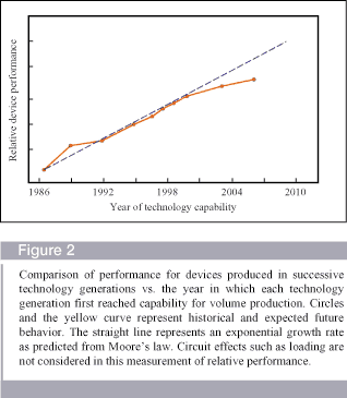 Figure
2
Figure
2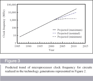 Figure
3
Figure
3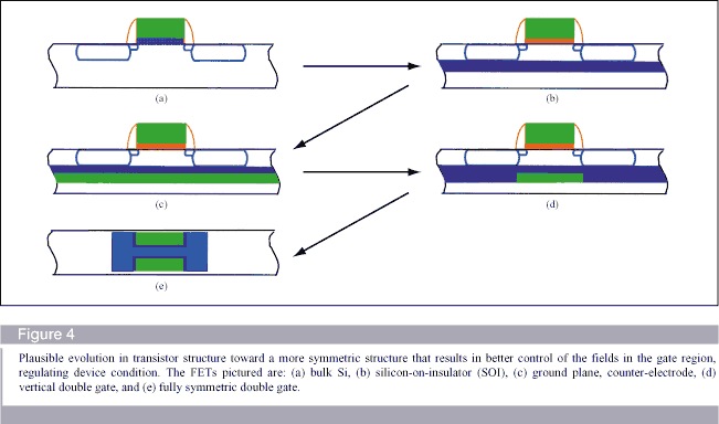 Figure
4
Figure
4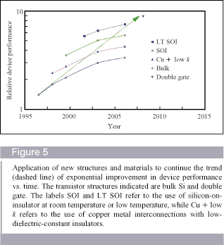 Figure
5
Figure
5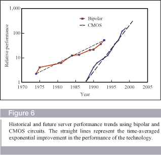 Figure
6
Figure
6