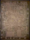
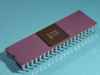
IC 4004: Internal structure
photo courtesy:
The antique chip collector's page.
Your resource to the fundamental assembly language programming . © 2004
An Evolution Of The Microprocessors .
Part I.
The First Generation.
|
4004 |
|
IC 4004: Internal structure photo courtesy: The antique chip collector's page. |
|
Designs Available : C4004, C4004 (Gray Dye), D4004, P4004 . Transistors : 2300, 16 pin DIP ( Dual Inline Package ). (Absolutely an obsolete number considering the architecture of the today's powerful processors.) clock speed : Introduced at 108KHz then subsequently upgraded to 500KHz and then later to 740KHz. Microns (size) : 10 microns. MIPS (Million Instructions Per Second) : 0.06. Addressable Memory : 640 Bytes. Bus Width : 4 bits. Interrupts : NA. stack : 4X12. I/O Ports : NA. Reg's index : 16 - 4 bit. Features : 45 Instructions. 1) C4004 - White/Gold CerDIP. 2) D4004 - Gray Ceramic DIP. 3) P4004 - Black/Gray Resin DIP. Typical Usage : BUSICOM calculator, Small Arithmetic Manipulations, Supported BCD. |
|
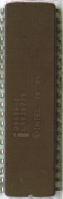
4040 |
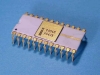
C4040 photo courtesy: The antique chip collector's page. |
|
Designs Available : C4040, D4040, P4040 . Transistors : > 2300, 24 pin DIP. clock speed : Introduced at 740KHz 2 phase. Microns (size) : More than twice as wide as the 4004. MIPS (Million Instructions Per Second) : > 0.06. Addressable Memory : 8 KB Program, 5 KB Data. Bus Width : 4 bits. Interrupts : NA. stack : 8X12. I/O Ports : NA. Reg's index : 24 - 4 bit. Features : 60 Instructions. 1) C4040 - White/Gold CerDIP. 2) D4040 - Gray Ceramic DIP. 3) P4040 - Black Resin DIP. Typical Usage :, Small Arithmetic Manipulations, Supported BCD,early game development,tests, early software development, small control systems. Supplimentary Chips : 4001 (ROM), 4002-1/2 (RAM), 4003 (shift register), 4008 (EPROM Interface), 4009 (EPROM Interface),4201 (Clock, Avail 1Q/75), 4207 (I/O), 4209 (I/O), 4211 (I/O), 4265, 4269, 4289 (System Memory Interface), 4308 (1K ROM),4702 (EEPROM), (4316 2K ROM), 4101 (128K RAM), 3216/3226 (4-bit Bus Driver). |
|
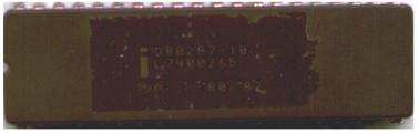
8008 |
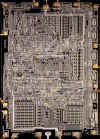 8008 internal structure. photo courtesy: The antique chip collector's page. |
|
Designs Available :( Originally code-named 1201) C8008, C8008-1, D8008, D8008-1. Transistors : 3500, 18 pin DIP. clock speed : Introduced at 200KHz then later upgraded to 800KHz. Microns (size) : 10 microns. MIPS (Million Instructions Per Second) : 0.06. Addressable Memory : 16 KB. Bus Width : 8 bits. Interrupts : Vectored, 8 Level. stack : 7X14. I/O Ports : NA. Reg's index : 6 - 8 bit. Features : 48 Instructions. 1) C8008 - Gray CerDIP. 2) C8008-1 Gray CerDIP. 3) D8008 - Gray Ceramic. 4) D8008-1 - Gray Ceramic. Architectures of the 4004 and the 8008 differed largely. Typical Usage :A base for the architecture of 8080, bottling machines, simple calculators, Data/Characters manipulations, the 8008 was to be single chip version of Control Terminal Corporation's (CTC) CPU design, which was to be implemented as TTL logic chips. |
|
8080 |
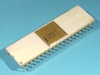
C8080-8 photo courtesy: The antique chip collector's page. chip construction : 8080 photo courtesy: Intel corporation ®. |
|
Designs Available : C8080, C8080 - 8, C8080A,C8080A - 1, C8080A - 2, D8080, D8080A, ID8080A, D8080A - 1, D8080A - 2, P8080A, P8080A 1, P8080A - 2, MD8080A/B ( Military Version ). Transistors : 6000, 40 pin DIP. clock speed : Introduced at 2MHz then later upgraded to 2.6MHz and then to 3MHz. Microns (size) : 6 microns. MIPS (Million Instructions Per Second) : 0.64. Addressable Memory : 64 KB. Bus Width : 8 bits Data Bus, 16 bits Address Bus. Interrupts : Vectored, Multi Level. stack : Stack Pointer. I/O Ports : 512. Reg's index : 6 - 8 bit. Features : 48 Instructions. 1) C8080, C8080 - 8, C8080A,C8080A - 1, C8080A - 2 White/Gold cerDIP. 2) D8080, D8080A, ID8080A, D8080A - 1, D8080A - 2 Gray Ceramic DIP . 3) P8080A, P8080A 1, P8080A - 2 Black Resin . 4) MD8080A/B ( Military Version ) Gray Ceramic DIP. Typical Usage :Traffic Light Controller, implemented in "Altair 8800" the first PC, ten times the higher performance as compared to 8008, six fundamental support chips. Supplimentary Chips : 8205 (Binary Decoder), 8212 (8-bit I/O Port), 8214 (Priority Interrupt Controller), 8216 (4-bit Parallel Bi-directional bus driver), 8224 (Clock generator), 8228 (System controller and bus driver), 8238 (System controller and bus driver (enhanced timing control)), 8251 (Communications Interface), 8253 (Programmable Interval Timer), 8255 (Programmable Peripheral Interface), 8257 (DMA Controller), 8259 (Interrupt Controller), 8271 (Floppy Disk Controller), 8273 (SDLC Protocol Controller), 8275 (CRT Controller), 8279 (Keyboard/Display Interface), 8801 (Clock Crystal for use with the 8224) |
|
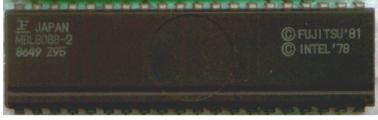
8085 |
C8085 photo courtesy: The antique chip collector's page. |
|
Designs Available : C8085, C8085A,C8085A - 2, C8085AH, C8085AH - 1, C8085AH - 2, D8085, D8085A - 2, D8085AH - 1, D8085AH -2, P8085A, P8085A - 2, P8085AH, P8085AH - 1, P8085AH - 2, ID8085A. Transistors : 6500, 40 pin DIP ( NMOS & HMOS CPU ). clock speed : Introduced at 3MHz then later upgraded to 5MHz and then to 6MHz. Microns (size) : 3 microns. MIPS (Million Instructions Per Second) : 0.37. Addressable Memory : 64 KB. Bus Width : 8 bits Data Bus, 16 bits Address Bus. Interrupts : 4 Vectored ( (RST 5.5 /6.5 /7.5), TRAP) 1 non-vectored ( INTR ), 8 software interrupts. stack : Stack Pointer. I/O Ports : NA. Reg's index : 6 - 8 bit. Features : 48 Instructions. 1) C8085, C8085A,C8085A - 2, C8085AH, C8085AH - 1, C8085AH - 2 Purple/Gold cerDIP. 2) D8085, D8085A - 2, D8085AH - 1, D8085AH -2 Gray Ceramic DIP . 3) P8085A, P8085A - 2, P8085AH, P8085AH - 1, P8085AH - 2 Black Resin . 4) ID8085A Gray Ceramic DIP. Typical Usage :Small home appliances, implemented in Stepper Motor Interface, DAC 0808 interfacing. Supplimentary Chips : 8155 (2048-bit static MOS RAM with I/O Ports and Timer, CE Active Low), 8156 (Same 8155, but CE Active High), 8355 (16,384-bit ROM with I/O), 8755 (16,384-bit EPROM with I/O), 8251A (Programmable Communications Interface), 8253-5 (Programmable Interval Timer), 8255-5 (Programmable Peripheral Interface), 8257-5 (DMA Controller), 8259-5 (Interrupt Controller), 8279-5 (Keyboard/Display Interface). |
Please visit "The antique chip collector's page" for more illustrations. The author has a priceless personal collection of the "first generation" chips.
The Second Generation.
|
8086 |
8086 : IC. |
|
Designs Available : Unknown. Transistors : 29000, 40 pin DIP. clock speed : Introduced at 5MHz then later upgraded to 8MHz and then to 10MHz. Microns (size) : 3 microns. MIPS (Million Instructions Per Second) : 0.33 MIPS, 0.66 MIPS, 0.75 MIPS respectively. Addressable Memory : 1 MB. Bus Width : 16 bits Bus. Interrupts : available. stack : Stack Pointer. I/O Ports : NA. Features : The Fundamental Processor for the TRUE computing. Typical Usage : Portable PC, Ten times higher performance as compared to 8080. |
|
8087 |
8087 : IC Math Co-processor. |
|
8088 |

8088 : Internal Structure. photo courtesy: Intel corporation ®. |
|
Designs Available : Unknown. Transistors : 29000, 40 pin DIP. clock speed : Introduced at 5MHz then later upgraded to 8MHz . Microns (size) : 3 microns. MIPS (Million Instructions Per Second) : 0.75 MIPS . Addressable Memory : 1 MB. Bus Width : Internal : 16 bits Bus, External : 8 bits Bus. Interrupts : available. stack : Stack Pointer. I/O Ports : NA. Features : Similar to 8086 except it's 8 bit External Bus. Typical Usage : Portable PC, It became a standard Processor for all IBM PCs and their Clones. |
8088 : Internal Structure. |
|
80186 |
Date of the release : 1982.
Designers : Unknown.
Typical Usage : Microcontroller Applications.
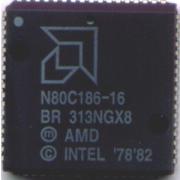
80186 : IC. |
|
80286 |
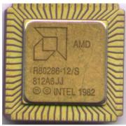
Advanced Micro Devices ( AMD ) 80286 : IC. 
80286 : Internal Structure. photo courtesy: Intel corporation ®. |
|
Designs Available : Unknown. Transistors : 1,34,000. clock speed : Introduced at 6MHz then later upgraded to 10MHz and susequently to 12MHz . Microns (size) : 1.5 microns. MIPS (Million Instructions Per Second) : 0.9 MIPS, 1.5 MIPS, 2.66 MIPS respectively. Addressable Memory : 16 MB, Virtual Memory 1GB. Bus Width : 16 bits Bus. Interrupts : available. stack : Stack Pointer. Features : The first processor to introduce the Protected Mode Programming ( All its predecessors had Real Mode Programming ). Typical Usage : It became a standard Processor for all IBM PCs and their Clones. |
The Third Generation.
|
80386 |
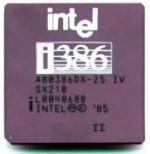
Intel386� DX CPU. photo courtesy: www.PCMECH.com®. 
80386 : Internal Structure. photo courtesy: Intel corporation ®. |
|
Designs Available : 80386DX, 80386SX, Intel386� SL CPU ( Specifically designed for portables. )
. Transistors : 80386DX / 80386SX : 275,000. 80386SL : 855,000. clock speed : 80386DX : Introduced at 16MHz then later upgraded to 20MHz, 25MHz and susequently to 33MHz . 80386SX : Introduced at 16MHz then later upgraded to 20MHz and susequently to 33MHz . 80386SL : Introduced at 20MHz then later upgraded to 25MHz. Microns (size) : 1.5 microns ( now 1 micron ). MIPS (Million Instructions Per Second) : 80386DX : 5, 6 - 7, 8.5, 11.4 MIPS( 9.4 SPECint92 on Compaq/i 16K L2) respectively. 80386SX : 2.5, 2.7, 2.9 MIPS respectively. 80386SL : 4.21, 5.3 MIPS respectively. Addressable Memory : 4 GB, Virtual Memory 64 TB. Bus Width : 80386DX 32 bits Bus. 80386SX Internal Bus : 32 bits Bus, External Bus : 16 bits Bus. 80386SL Internal Bus : 32 bits Bus, External Bus : 16 bits Bus. Interrupts : available. stack : Stack Pointer. Features : The first 32 bit processor to introduce the Protected Mode Programming and completely compatible with previous 80x86 processors. It also introduced two new registers. Typical Usage : 80386DX : Desktop computing made faster. 80386SX : Entry - level desktop, The foundation of the true portable computing. 80386SL : Portable PCs made reality, Includes cache, bus, memory controllers. |
|
80486 |
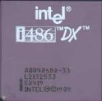
Intel 80486 : IC. photo courtesy: www.PCMECH.com. 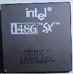
Intel 80486 : IC. photo courtesy: Computer Craft - This Old 486. 
80486 : Internal Structure. photo courtesy: Intel corporation ®. |
Intel486� DX2 CPU
MAR 3, 1992. ( 50 MHz )
AUG 10, 1992. ( 66 MHz )
Intel486� SL CPU
NOV 9, 1992. ( 20 MHz, 25 MHz, 33MHz)
Intel486� DX4 CPU
MAR 7, 1994. ( 75 MHz, 100 MHz )
|
Designs Available : Intel486� DX CPU, Intel486� SX CPU, Intel486� DX2 CPU, Intel486� SL CPU, Intel486� DX4 CPU
. Transistors : 80486DX : 1,200,000. 80486SX : 1,185,000. 80486DX2 : 1,200,000. 80486SL : 1,400,000. 80486DX4 : 1,600,000. clock speed : 80486DX : Introduced at 25MHz then later upgraded to 33MHz and susequently to 50MHz . 80486SX : Introduced at 16MHz then later upgraded to 20MHz,25MHz and susequently to 33MHz . 80486DX2 : Introduced at 50MHz then later upgraded to 66MHz. 80486SL: Introduced at 20MHz then later upgraded to 25MHz and susequently to 33MHz . 80486DX4 : Introduced at 75MHz then later upgraded to 100MHz . Microns (size) : 0.8 microns ( 0.6 microns - 80486DX4 ). MIPS (Million Instructions Per Second) : 80486DX : 20 MIPS, 16.8 SPECint92, 7.40 SPECfp92, 27 MIPS, 22.4 SPECint92 on Micronics M4P 128K L2, 41 MIPS, 33.4 SPECint92, 14.5 SPECfp92 on Compaq/50L 256K L2 respectively. 80486SX : 13 MIPS, 16.5 MIPS, 20 MIPS, 12 SPECint92, 27 MIPS, 15.86 SPECint92 respectively. 80486DX2 : 41 MIPS, 29.9 SPECint92, 14.2 SPECfp92 on Micronics M4P 256K L2; 54 MIPS, 39.6 SPECint92, 18.8 SPECfp92 on Micronics M4P 256K L2 respectively. 80486SL : 15.4, 19, 25 MIPS respectively. 80486DX4 : 53 MIPS, 41.3 SPECint92, 20.1 SPECfp92 on Micronics M4P 256K L2; 70.7 MIPS, 54.59 SPECint92, 26.91 SPECfp92 on Micronics M4P 256K L2 respectively. 80486DX4 : Addressable Memory : 4 GB, Virtual Memory 64 TB. Bus Width : 32 bits Bus. 80486SL : ( Both internal data path and external data patch : 32 bits) Interrupts : available. stack : Stack Pointer. Features : The last numbered copyrighted 32 bit processor .Like 80386 it is also completely compatible with previous 80x86 processors. It introduced the concept of the pipeline. Typical Usage : 80486DX : Extensively implemented in the first servers. 80486SX : Devoid of the 80x87 math co-processor. Harnessed in the embeded technology. 80486DX2 :Introduced " Speed Doubler Technology" where the CPU core ran twice the speed of the bus. 80486SL : Exclusively designed for the Note book PCs . 80486DX4 : Speedy applications, the initial 3d graphics experimentation. |
References : www.i-probe.com, The antique chip collector's page.
Next : An Evolution Of Intel Microprocessors - Part II.
|
PREVIOUS |
|
NEXT |
© 2004 by Pratik.M.Tambe.
|
| PRIMITIVEASM© |