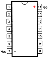
14-pin and 16-pin IC pin numbers
[ Español ]
This section contains schematics to build a programmable timer. If you wish to download this project for offline viewing, please download this ZIP file: Timer project
This project consists of a digital clock and an electronic switch or relay controlled by the clock. This switch will activate or deactivate at user-programmed times, with only one time interval available. Due to its complexity there are no plans to add any more features, instead a CPLD version of this project may be developed some day with more advanced functions.
This design uses only standard CMOS logic chips widely available in any electronics store. It has been designed to operate from battery power thus it has a very small power consumption. It can run from 3V to 18V.
I've divided schematics in parts that implement specific functions and can be understood separately. Each schematic presented below has the proper references to external nodes so there will be no confusion to interconnect these parts. I've built and thoroughly tested these circuits.
Below you will find explanations for each presented circuit. However you don't need to understand them to build and use this project. You only need good soldering skills.
Do not forget supplies to all integrated circuits (ICs) used in this project. Supplies are not indicated in the schematics but each IC needs them. For 14 pin ICs, supply positive to pin 14 and ground (negative) to pin 7, for 16 pin ICs supply positive to pin 16 and ground to pin 8. Always take care of proper pin numbering order:
This circuit can work from 3V to 18V. Make sure the capacitor used in the reset circuit is rated up to at least the voltage supplied. Resistor used for led displays is calculated for 5V operation, for higher voltages you should use higher values (see display section).
Be careful when managing these ICs because they are sensitive to Electrical Static Discharge (ESD). You should keep them packeted in a conductive foam while not mounted to minimize risk of damage.
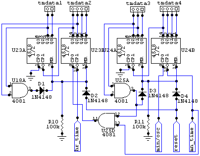
The heart of this design are three counters/registers blocks that keep current time and user-programmed start and end times. This is implemented using 4518 ICs. As you can see from the schematics below I use 4081 AND gates and 1N4148 diodes (used as OR gates) to design the circuitry that will generate the proper reset signals so that minutes return from 59 to 00 and hours from 23 to 00.
Notice inside every 4518 there are two independent counters, this way we can reduce the amount of chips needed. One 4518 chip is identified by its part number (e. g. U23, U24, ...) while the ending letter (A, B) identifies which one of the counters it refers to inside a chip. Thus parts U23A and U23B are the same IC, notice their pin numbers are different. This part ID convention is used in all circuits in this page.
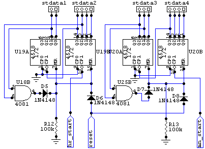
4518 is a decimal counter, decimal meaning it counts from 0 to 9 as opposite to a binary counter that counts from 0 to 15. This way we already have minute units, that is U20B. Next step is the tens of minutes digit, it will have to count from 0 to 5 and is U20A. It is increased by one every time minute units reset from 9 to 0. For this purpose we use inverted clock signal input, pin 2, that will increment the counter in the falling edge, this is ideal since this is exactly what the fourth bit from U20B (pin 14) does when counts from 9 to 0. This would count from 00 to 99 but we want it to go back to 00 when it reaches 60, to achieve this we include U25B, output from this AND gate will be logic 1 when a 6 is output from U20A (notice 6 is the first number to have two logic 1 in the 2nd and 3rd bits (pins 4 and 5). When that AND gate outputs a logic 1 it resets both counters to 00 through their asynchronous reset inputs (pins 7 and 15 of U20). Diodes D7 and D8 implement an OR gate so that counters can be reset either from the described AND gate output or from external reset input. Resistor R13 keeps these reset inputs low when both inputs to D7 and D8 are low (otherwise it would be in high impedance state since D7 and D8 are not conducting).
So far we have a counter from 00 to 59 (U20). The same idea is used to implement an hours counter counting from 00 to 23. AND gate U18B will output logic 1 when counter U19A contains a 2 and U19B a 4 (at 24 it'll immediately reset the counters to 00 so that after 23 the user sees 00).
Inputs hr_start and mn_start allow to set hour and minute values respectively so the timer switch activation time is programmable. Set time is available at outputs stdata and will be displayed in a 7-segment led display. Reset input is used to reset the time to 00:00.
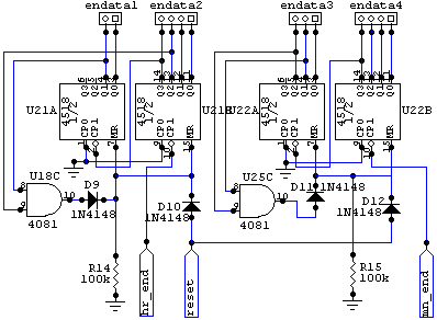
This end register is identical to the start register.
This time register is almost identical but it includes an additional wire to add one hour when minutes reset from 59 to 00. This way it behaves like a real digital clock. AND gate U25D disables that signal when the mn_time is low (i. e. the minute button is pressed) so that when the user is setting the time the hours register will not increase when going from 59 to 00 minutes. It also receives a pulse every minute in the 'min/osc' input so it is a real clock.
Some of you might think there could be glitches resetting counters before they should, well I thought about it and decided to try and build the circuit to see if that would be a problem. Well, in fact it is not, the circuit works perfectly as is.
To generate the 'min/osc' pulse every minute a quartz crystal oscillator is used:
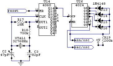
XTAL1 quartz crystal oscillates at 32768 Hz driven by an inverting buffer in U14, this IC also divides this down to 2 Hz and 4024 (binary counter) further divides down to 1 Hz and 1 pulse/minute. U26 forms a 0 to 119 counter, since it receives a 2 Hz signal it will count from 0 to 120 in exactly one minute. Diodes D13, D14, D15, D16 and resistor R19 form a 4-input AND gate that will output logic 1 when U26 reaches 120 as this is "1111000" in binary and will reset the counter to 0 and provide a pulse to the min/osc output. The sec/osc output will give a pulse every second.
As important as these circuits described above is a display circuit so the user can see the contents of these counters and set them. The following circuit performs this task.
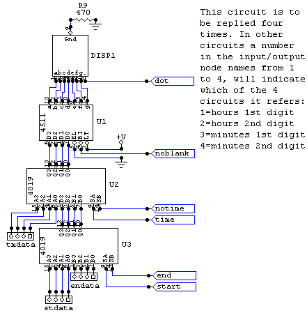
Note this circuit has to be replied four times, one for each digit to be displayed. Node names have a number appended in other circuit nodes that tells which digit they connect to:
4511 is a decimal to 7-segment converter and led driver. It'll lit the proper leds to display the number entered in binary form on pins 7, 1, 2 and 6. 4019 are selectors and choose which of the three inputs is brought to the 4511. They are used to select which register (time, start and end) is displayed.
An important consideration is resistor R9 value. 470 ohm is suggested for operation at 5V for a typical display. If you believe your display is dark at your definitive operating voltage, decrease its value. If you wish to lower brightness to reduce power draw then increase its value. Relation current/brightness depends on your particular display. As a rule of thumb, ideal value is the highest one that satisfies the user. Higher value means less power draw, and if operating from batteries this is an important issue.
Here is a circuit that generates those control signals seen above to select which register is displayed. It is simply a bit-shifter controlled by a push-buttton.
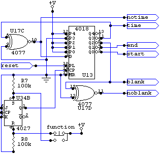
It is designed around a 4018 IC universal shift register. XNOR gates are used as inverters here, the reason is that we need two of these gates in another circuit and the remaining two would be otherwise unused (there are four in a 4077 IC). U34B acts as a push-button de-bouncer, this was also an unused part from another circuit. Many thanks go to Stefan Krommes who helped me solve push-button bouncing problems.
As you can see we load a binary pattern to the 4018 through its parallel inputs at start-up using the reset signal. This pattern is "0111", as the outputs are inverted the output will be "1000", the 1 is initially set to the 'time' output so at turn on time register will be shown on the display. Pushing the function button the 1 will rotate one position and will enable the start register, pushing again will enable the end register and again the 'blank' output. This output is inverted using U17D to generate 'noblank', with this signal logic 0 it will blank the led displays to save power. Pushing again it'll go back to 'time' and so on. The reason for this electronic selector instead of a mechanical selector is the fact a push-button and a 4018 are cheaper and provide a nice interface.
Well, so far what about the buttons to set those counters seen at the beginning? Here is the circuit that uses control signals generated in the previous circuit to decide what counter is active on the display and thus what counter the minute/hour buttons have effect on.
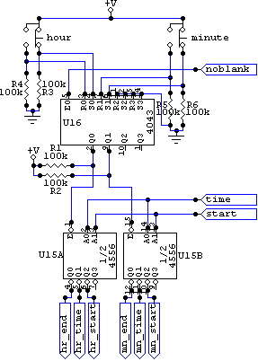
This circuit has R-S latches (U16) that work as push de-bouncers. It uses their enable inputs to disable buttons when display is off. U15 is a decoder, but in this circuit we can think of it as a selector, it chooses according to the control signals the path push-button signals will follow.
An important signal as we have seen is a reset signal. When this circuit is powered up many elements need a pulse to set up themselves, since sequential logic starts in an unknown state. To generate this pulse this simple circuit works fine:
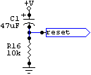
At start up capacitor C1 is discharged thus 'reset' node is at positive supply potential as no voltage drop exists in a discharged capacitor. As C1 charges through R16, its voltage drop increases and node 'reset' goes down to ground voltage. Well, this reset signal is not exactly square but works correctly.
This is one of the most important circuits in this project. This circuit reads contents of time, start and end registers described previously and decides whether an electronic switch has to be enabled or disabled.
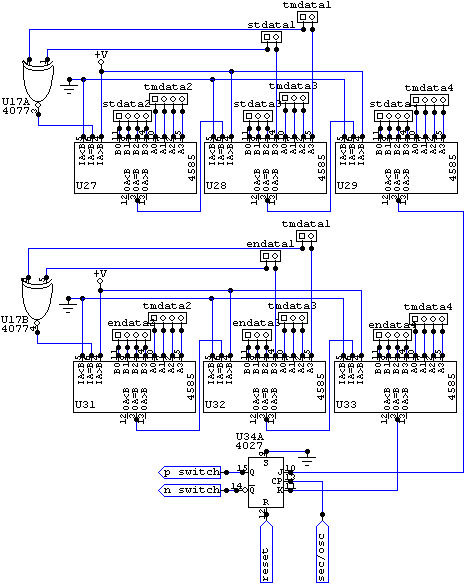
The 4585 is an universal magnitude comparator, here used only to tell if the compared values are equal or not. As you can see there are two horizontal rows of ICs, the first row compares current time against start time register and the second row compares current time against end time register. When current time matches start time, U34A J-K flip-flop will be set (logical 1). When current time matches end time, J-K flop-flop will be reset (logical 0). If start and end times are set at the same time, the switch will be enabled and disabled continually during that minute at a rate of 1 blink/second.
This control circuit however may generate wrong output at the time the registers are being set by the user. I haven't given a way to correct for this, just wait after 24 hours it'll set up correctly by itself.
There is an unused AND gate you should take care of.

Unused parts with unconnected inputs may oscillate or bias themselves into intermediate states and waste power. To avoid this from happening these inputs must be wired to ground or supply, I have decided to wire them to supply because it is available on pin 14 and all it needs is to solder together pins 12, 13 and 14. Make sure pin 11 is not connected (unused outputs must be left unconnected).
In this section I present some common circuits to control various loads. Of course other circuits can be used to suit specific needs as long as they can be driven from the timer switching signal and supply if required. The timer control outputs are low current CMOS signals available at pins 14 and 15 of U34A (labeled n switch and p switch in Electronic switch control schematic), active low and active high respectively. Keep in mind these outputs can source no more than 1 mA depending on the particular chip used (see its datasheet).
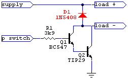
This single transistor circuit is suitable if the load you intend to control runs from a low voltage DC supply up to 45V and draws less than 100 mA of current. The load supply (labeled supply) can be the same as the timer supply or another as long as it does not exceed the maximum transistor collector-emitter voltage (45V for BC547). Also remember it does not provide isolation, both timer and load share the same ground.
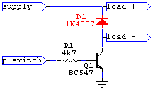
You can replace the transistor by a BC109 or BC547BP to increase available current to 200 mA. BC109 supports only up to 20V. The red diode is optional and must be placed if the load is inductive (for example a relay coil) to absorb the spike generated at turn off. This circuit can be used to drive a relay coil to control higher currents however if you run the timer from batteries keep in mind the relay will drain them quickly if active for long periods of time.
The small current provided by the timer CMOS output is sufficient to switch a BC547 transistor. With a minimum gain of 150 a base current of 1 mA is enough to let 100 mA through the transistor to the load well within its saturation region. BC109 or BC547BP have a minimum gain of 200 and support a current of 200 mA.
You can add a second transistor to increase current capability up to 1 A:
This configuration is known as Darlington pair. The first transistor amplifies a very small current (1 mA) enough to polarize the second transistor with more current and allow it to carry up to 1 A. To switch high currents the TIP29 transistor requires a heat sink as it can dissipate up to 1W of power. With this circuit there will a be a voltage drop of 0.9V in Q2.
A known drawback of this circuit is that power transistor Q2 will dissipate a considerable amount of heat because it is not fully saturated. For supply voltages up to 14V this can be improved with this variant:
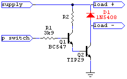
In this circuit current to polarize Q2 is taken directly from the supply instead of the power transistor collector, this way the transistor will always be fully polarized regardless of the collector voltage. The drawback now is the current taken to polarize Q2 is not part of the load current thus the circuit itself takes additional power from the supply. Yet because Q2 is fully saturated with a voltage drop of 0.2V, more voltage is available to the load and less wasted as heat, this better efficiency compensates the additional power drawn. For 14V or higher voltages the power dissipated at resistor R2 exceeds the power dissipated at Q2 in the Two transistor I Darlington pair circuit, in this case the mentioned circuit should be used instead.
Resistor R2 value depends on the supply voltage and can be calculated with the following formula:
R2 (ohms) = (supply voltage − 0.9) / 0.07
This resistor can dissipate 1 watt of power, so use a properly sized resistor.
The following circuit is a solid state switch based on a Triac. It can be used to switch mains loads (works only with AC currents), takes 3 to 6 mA of current from the timer supply and provides isolation so the timer circuits will not be at mains dangerous voltages. Operate and test this circuit with care as it is under dangerous mains voltages.
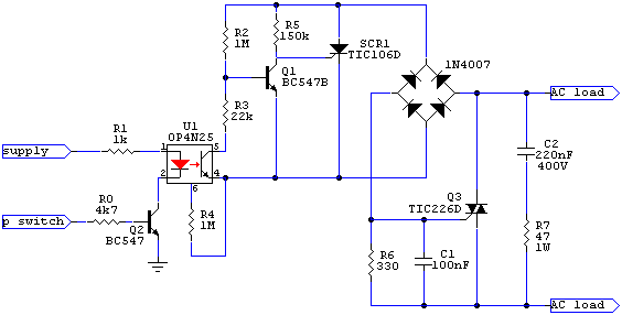
Nodes AC load must be connected like a switch, between mains and load. Node supply is the timer supply (DC between 3V and 18V) and note that only Q2 collector connects to timer ground and nothing else in this circuit.
This circuit can control up to 8 amps of current. The triac requires a heat sink depending on the current you intend to control, it can dissipate up to 14 W of heat at 8 amps that results in a heat sink capable of 5.5 °C/W. When off there is a small leakage current, never touch the output even if it is off.
U1 optocoupler provides mains isolation and passes through the activation signal from isolated timer circuits to live mains circuit. R1 limits current to the optocoupler led, when activated, the optocoupler transistor shorts to ground the weak polarization current that kept Q1 active. Current through R5 is no longer shunt to ground and fires the SCR that shorts the bridge rectifier output, now current through the bridge is high enough to create a voltage drop in R6, charge capacitor C1 and fire the Triac. Then the Triac will bridge the AC load terminals conneting to load to the mains. C2 and R7 form a snubber network. The triac may not turn off properly for loads under 60 mA.
When operating this circuit from batteries it is very important to turn off its display (pressing the select button until display blanks out) when not needed. It places a huge current draw that will discharge the batteries quickly. These are measured current values at 5V:
I have used it to switch on and off automatically our Christmas tree lights and also as an alarm-clock.
Project completed on August 2002.
Copyright © 2002 Jeroni Paul.