| Power Supplies | ||
|
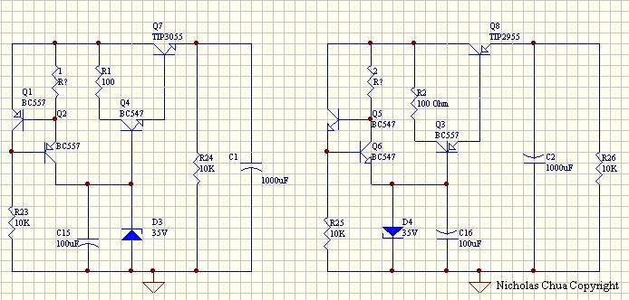
CCS Zener Diode Regulation Questions to |
CCS ZENER DIODE REGULATION
The value of R1 and R2 is given by 0.7/R=current set where 5ma should be suffice for the zener. Q1 and Q2 are cc source and sink for q 5 and 6 . Q3 and Q4 just form a a Darlington configuration. This increase the gain of the pair as the hfe for the Q4*Q7 is much higher than any one alone. However resistance is used to limit the number of current flowing thru the q4 to avoid overloading the q4. Because gain is much higher, the base current needed to be source for the zener would be less, Ie/hfe =Ib. Also with the the high amount of gain, the power supply is inherently more stable as the poles of the ps is shifter much much further away from the 180 out of phase. The cap is just further moves the pole further from 180 out of phase. Quality or Q factor, ESR of caps are not so critical as mention, the ps is stable without the cap compensation. However the vreg is off a high drop rate and is not very ideal but simplicity is there and is much easier to build than LDO which I prefer. V drop out is easily calculated by adding 0.7*2 (to compensate Q4 and Q7) + Minimum voltage for the zeners to regulated +which also includes the minimum voltage drop across ccs which is 0.7v. As mention parts can be changed where the Q and ESR is not very crucial for stability unlike LDO type. you could opt for better premium parts or lower capacitance or higher but try not to exceed 4700uf. Also not drawn in the schematic is the need for diode protection similar to the 317 methods. This is to prevent current flowing back into the transistors and spoiling them. Power dissipation is given by Vin-Vout/Current thru the Vreg. Heat sink type and thermal rating would follow the dissipation needed.
|