| Building The RAT_1 A Step by Step Guide. | ||||||||||||||||||||||||||||||||||||||||||||||||||||||||||||||||||||||
| The following two pages will show you how to build up the RAT_1 Kit and then test it. | ||||||||||||||||||||||||||||||||||||||||||||||||||||||||||||||||||||||
|
||||||||||||||||||||||||||||||||||||||||||||||||||||||||||||||||||||||
![]() |
||||||||||||||||||||||||||||||||||||||||||||||||||||||||||||||||||||||
| First you will need a few tools: 
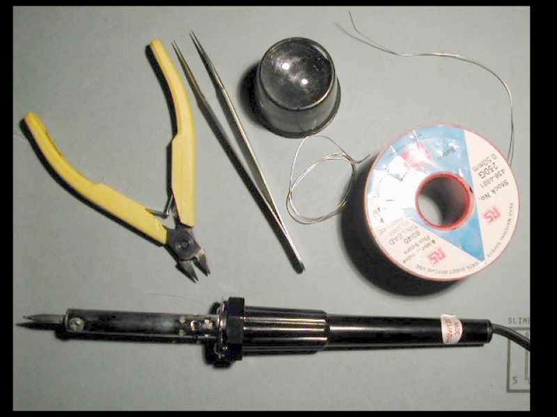
1. A fine soldering iron 15 to 30W 2. Resin cored solder 26swg 3. Side cutters 4. Tweezers 5 Perhaps a magnifying glass. The pcb is built up in stages determined by the height of the component. Low lying resistors and diodes first, then transistors, capacitors and the really big stuff, such as connectors, are fitted last. |
||||||||||||||||||||||||||||||||||||||||||||||||||||||||||||||||||||||
![]() |
||||||||||||||||||||||||||||||||||||||||||||||||||||||||||||||||||||||
| Ensure that you have all the components ready. 
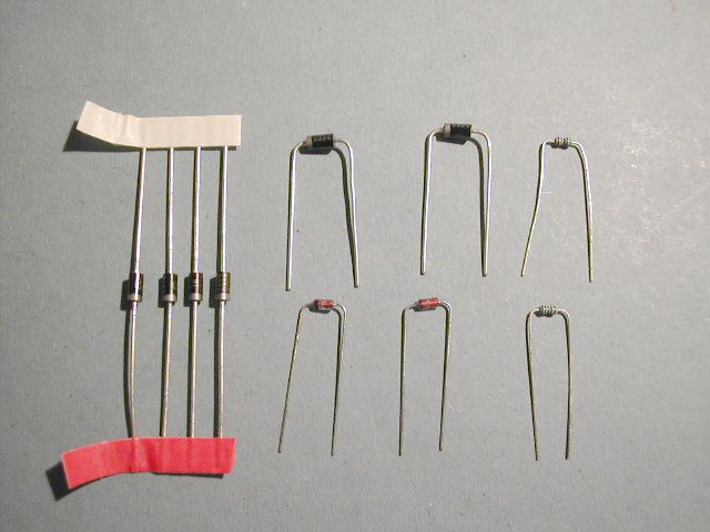
Sort them out into resistors, diodes, capacitors, transistors etc. Resistors have been labelled to make reading their value much easier. The resistors and diodes will have to be bent to go into the board. This is best done by grasping the component between thumb and forefinger, positioning the thumbnail 3mm from the end of the component body, then bend the component lead over the thumbnail at 90 degrees. It may take a little practice to get the knack. |
||||||||||||||||||||||||||||||||||||||||||||||||||||||||||||||||||||||
![]() |
||||||||||||||||||||||||||||||||||||||||||||||||||||||||||||||||||||||
| Step 1. 
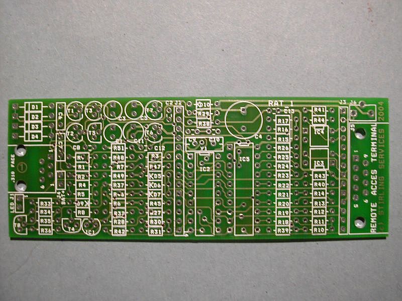
Start with the bare PCB. Identify the main components. Use the layout sheet contained in the rat_pack to assist finding the component location. Familiarise yourself with the orientation of the polarised components such as diodes, transistors, electrolytic capacitors and ICs. |
||||||||||||||||||||||||||||||||||||||||||||||||||||||||||||||||||||||
| Step 2. 
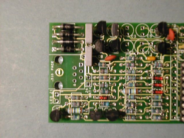
Now begin by fitting all the resistors and diodes Start with the components in the order they appear on the parts list. Bend the resistor leads so that they are the correct pitch for the holes in the board. Insert no more than 10 components at a time and solder from the reverse side of the PCB. Crop the excess component leads close to the board with sidecutters after soldering. 
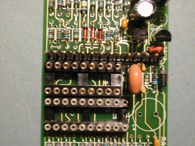
Make sure you fit the diodes and zeners in the correct way around. Check D9 carefully |
||||||||||||||||||||||||||||||||||||||||||||||||||||||||||||||||||||||
![]() |
||||||||||||||||||||||||||||||||||||||||||||||||||||||||||||||||||||||
![]() |
||||||||||||||||||||||||||||||||||||||||||||||||||||||||||||||||||||||
| Step 3. 
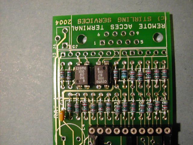
Now fit the two opto-isolators IC3 and IC4. Note that IC3 is fitted "upside down" compared to IC4. 
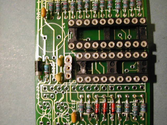
Fit the 18 pin DIL socket for the PIC and the 20 way socket for IC5. Fit the 3 pin piece of SIL socket for the crystal resonator - below. |
||||||||||||||||||||||||||||||||||||||||||||||||||||||||||||||||||||||
![]() |
||||||||||||||||||||||||||||||||||||||||||||||||||||||||||||||||||||||
![]() |
||||||||||||||||||||||||||||||||||||||||||||||||||||||||||||||||||||||
| The board should now look like this. | ||||||||||||||||||||||||||||||||||||||||||||||||||||||||||||||||||||||
| Step 4. 
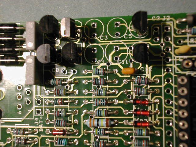
Now start fitting the small capacitors C2, C8, are 10nF C9, C10, are 22pF C12 and C13 are 100nF. |
||||||||||||||||||||||||||||||||||||||||||||||||||||||||||||||||||||||
![]() |
||||||||||||||||||||||||||||||||||||||||||||||||||||||||||||||||||||||
![]() |
||||||||||||||||||||||||||||||||||||||||||||||||||||||||||||||||||||||
| Step 5 
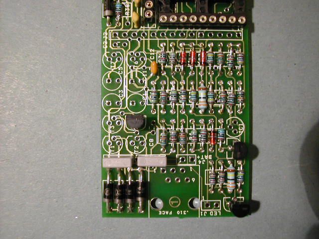
Now fit the 250V 10nF capacitors C6 and C7 next to the bridge rectifer (D1-D4). 
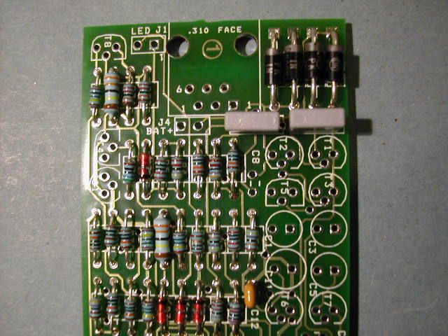
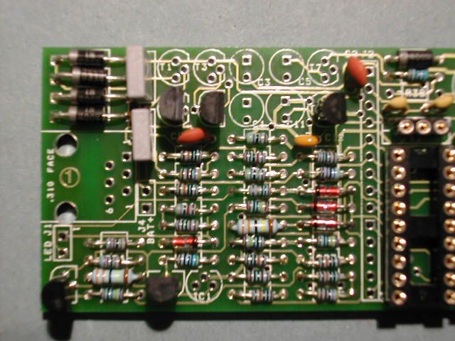
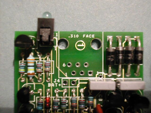
You can see from this photo the direction of the diodes and zener diodes. It is worth checking carefully at this stage. All diodes and zeners except D9 have their cathode bands facing the LED end of the board. |
||||||||||||||||||||||||||||||||||||||||||||||||||||||||||||||||||||||
| Step 6. Next we start to insert the transistors. It helps if you bend the middle leg forward before insertion. First sort out the 9 devices: 3 off BC847A General Purpose T4, T5, T8 2 off MPSA42 High Voltage NPN T2, T6 2 off MPSA92 High Voltage PNP T1, T7 1 off ZTX651 High Current NPN T3 1 off HT7533 or TC553302 3.3V voltage regulator. |
||||||||||||||||||||||||||||||||||||||||||||||||||||||||||||||||||||||
![]() |
||||||||||||||||||||||||||||||||||||||||||||||||||||||||||||||||||||||
| Fit the BC547 devices first into positions T4, T5 and T8. Check the orientation from the legend. Use the caps C6 and C7 as a guide to set the height of the transistors above the pcb - about 7mm or 0.25" |
||||||||||||||||||||||||||||||||||||||||||||||||||||||||||||||||||||||
![]() |
||||||||||||||||||||||||||||||||||||||||||||||||||||||||||||||||||||||
| Step 7. Continue to fit the MPSA42 parts T2 and T6 |
||||||||||||||||||||||||||||||||||||||||||||||||||||||||||||||||||||||
![]() |
||||||||||||||||||||||||||||||||||||||||||||||||||||||||||||||||||||||
| Step 8. Then fit the MPSA92 devices T1 and T7. They are fitted closest to the top edge of the board. Finally fit T3, noting that it is in a silver E-Line package and should be fitted with its curved side facing the diodes D1 to D4. |
||||||||||||||||||||||||||||||||||||||||||||||||||||||||||||||||||||||
![]() |
Step 9. Fit the voltage regulator IC1 next to T4. This can either be a Holtek HT7533 or Microchip TC553302 device. Ensure this device is inserted correctly. |
|||||||||||||||||||||||||||||||||||||||||||||||||||||||||||||||||||||
| Step 10. 
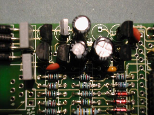
Now fit the electrolytic capacitors C1, C3 & C11, making sure that the +ve lead goes to the square pad in the pcb. |
||||||||||||||||||||||||||||||||||||||||||||||||||||||||||||||||||||||
![]() |
||||||||||||||||||||||||||||||||||||||||||||||||||||||||||||||||||||||
![]() |
||||||||||||||||||||||||||||||||||||||||||||||||||||||||||||||||||||||
| Step 11. Fit the LED. It may be in a plastic holder like this one or just a plain LED. The anode or +ve goes to the square pad on the pcb. |
||||||||||||||||||||||||||||||||||||||||||||||||||||||||||||||||||||||
![]() |
||||||||||||||||||||||||||||||||||||||||||||||||||||||||||||||||||||||
| Step 12. 
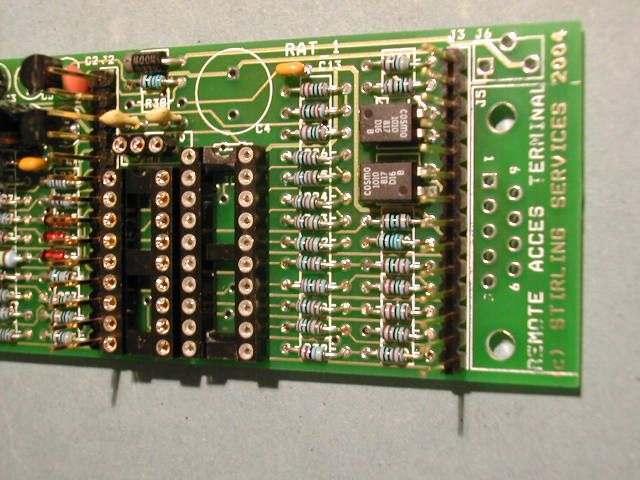
Fit the expansion headers J2 and J3 ensuring that they are set vertically upright. |
||||||||||||||||||||||||||||||||||||||||||||||||||||||||||||||||||||||
![]() |
Step 13. 
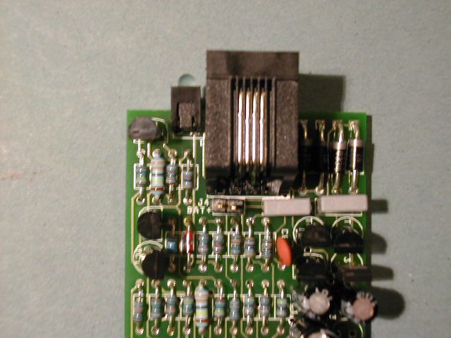
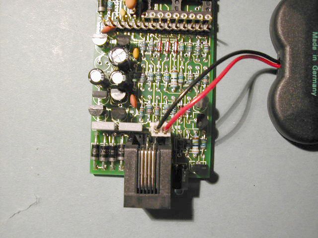
Fit the RJ11 phone line connector and the 2 pin header for the battery connection. |
|||||||||||||||||||||||||||||||||||||||||||||||||||||||||||||||||||||
![]() |
||||||||||||||||||||||||||||||||||||||||||||||||||||||||||||||||||||||
| Step 14. 
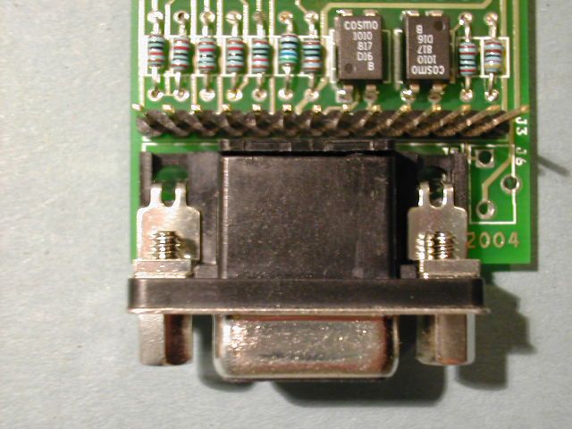
Fit the DB9 connector for the PC_Link It has two metal lugs that need a lot of solder to fix them to the board. |
||||||||||||||||||||||||||||||||||||||||||||||||||||||||||||||||||||||
![]() |
||||||||||||||||||||||||||||||||||||||||||||||||||||||||||||||||||||||
| Step 15 Plug in the ceramic resonator into the SIL socket. |
||||||||||||||||||||||||||||||||||||||||||||||||||||||||||||||||||||||
![]() |
||||||||||||||||||||||||||||||||||||||||||||||||||||||||||||||||||||||
| Now have a break! 
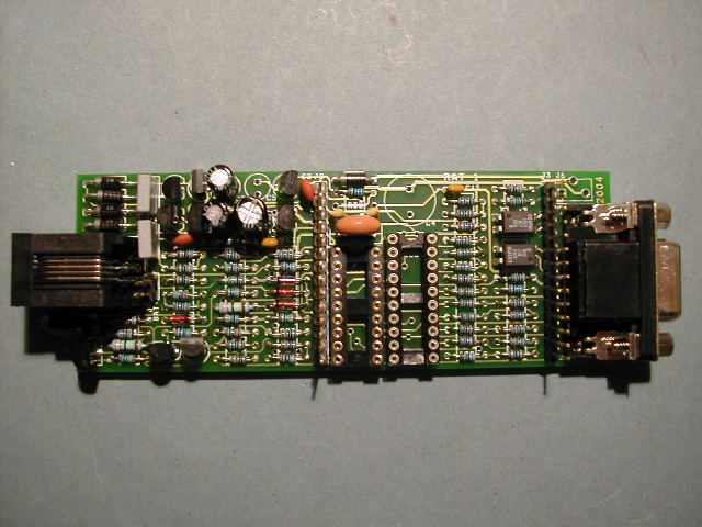
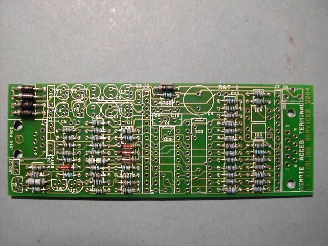
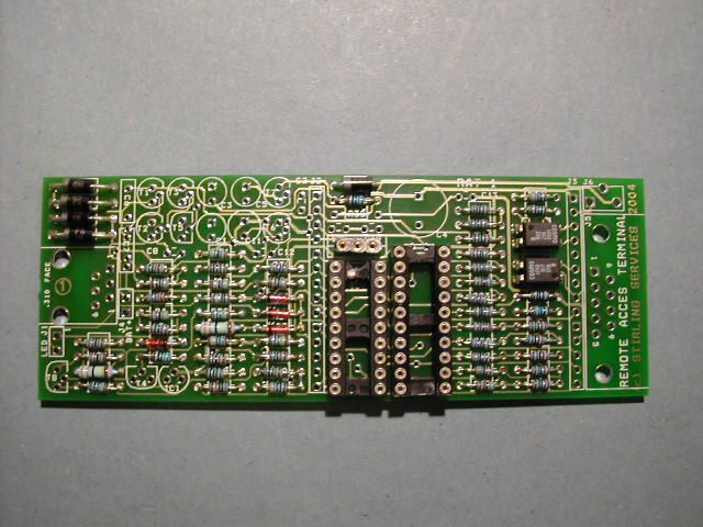
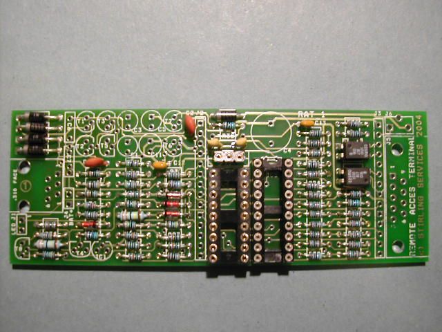
Your RAT_1 should now look like this! |
||||||||||||||||||||||||||||||||||||||||||||||||||||||||||||||||||||||
| Step 16 Finished (Almost!) 
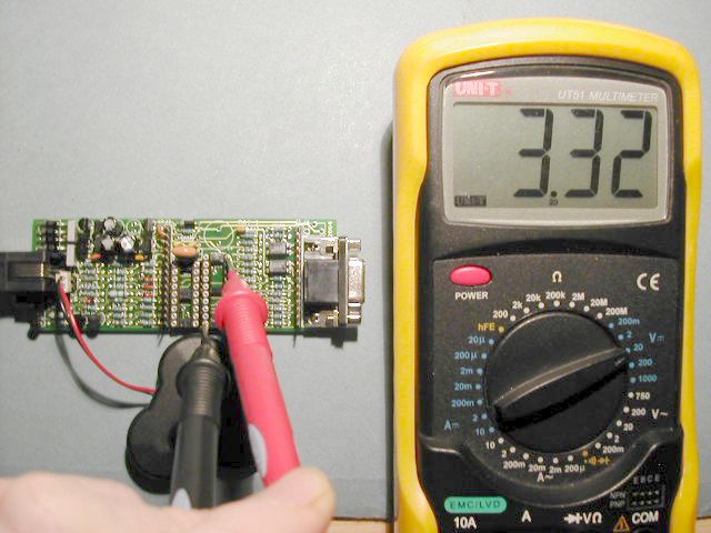
The RAT_1 is now ready for testing. Do NOT fit the PIC16F88 yet. 
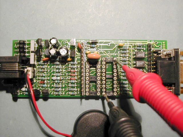
Check the pcb carefully before plugging in the battery. Make sure the battery is plugged in correctly!! |
||||||||||||||||||||||||||||||||||||||||||||||||||||||||||||||||||||||
![]() |
||||||||||||||||||||||||||||||||||||||||||||||||||||||||||||||||||||||
| We now use a DVM (multimeter) to check that there is 3.3V coming from the regulator. Put the probes on Pin 10 and Pin 20 of IC5 as shown. Also check that the battery voltage is about 3.6V or else the battery may need to be charged. |
||||||||||||||||||||||||||||||||||||||||||||||||||||||||||||||||||||||
![]() |
||||||||||||||||||||||||||||||||||||||||||||||||||||||||||||||||||||||
![]() |
||||||||||||||||||||||||||||||||||||||||||||||||||||||||||||||||||||||
| Go to the next page to continue testing RAT_1 | ||||||||||||||||||||||||||||||||||||||||||||||||||||||||||||||||||||||
| All text tnformation, photographs and design of this page, the rat_ring name in lower case text with underscore, Remote Access Terminal, RAT_1, use of the RAT acronym and downloads remain the sole property of Stirling Services. Others may gain automatic licence to use the RAT_1 design by purchasing the RAT_1 PCB from Stirling Services. | ||||||||||||||||||||||||||||||||||||||||||||||||||||||||||||||||||||||
| BACK TO PAGE 1 | ||||||||||||||||||||||||||||||||||||||||||||||||||||||||||||||||||||||