
Schematic of power test circuit
Overview
In this paper a short explaination of the design problem for power supply networks for high performance PLDs is given. A new approach to measure the frequency response is given. Practical measurements are presented.
Introduction
PLDs are becomming more and more a main part in modern electronis. The parts are getting bigger, faster and more powerful by the day. And so does the power consumption. Althrough the power/gate is decreasing by use of better technology and smaller geometry, the clock frequency is increasing as well as the number of gates per device. With increasing switching speed, the power supply becomes a critical part in the system design. The power supply network must be a low impedance source over a very wide range of frequencies. Otherwise ringing, dropouts and spikes on VCC/GND can disturb the function of the PLD, caused by the rapid changing power requirements of the PLD.
Broadband decoupling is teamwork
The power regulator must provide the DC current component to the power network. At maximum power and maximum ambient temperature, the regulator must be still full functional without overheating, clipping etc. . It's duty is also to react on low frequency power steps (DC..30kHz).
Middle frequency power steps can't be supplied by the regulator (he's too slow), they must be provided by high value capacitors (470...4700uF) either electrolytic or tantalum types. These capacitor can supply power to the PLD up to serval MHz, then the parasitic series inductance and resistance (ESL and ESR) increases the reactance of the capacitor and makes it useless.
Now its time for the small ceramic caps, typical 100nF/10nF. They come in small SMT packages (0805, 0603 or smaller) with low parasitic inductance. They can deliver currents up to serval hundred MHz an provide a low impedance source for high frequency currents.
But for the REALLY high speed switching devices, also this ceramic capacitors are not sufficient for power decoupling. Here is the need for power plane capacitance, which is formed by the ground plane and VCC plane of the multilayer board. To achieve a maximum of capacitance, a thin dielectric between the planes with a high K-factor and low loss factor should be used. Also 1 via per VCC/GND pin should be used to reduce parasitic inductance, NOT just one for two or more VCC/GND pins. BGA packages provide additional shorter connections from the board to the die, but are more difficult to handle (layout and soldering).
The Classic Approach
There are a lot of theories and application notes about power decoupling. Some just go for a brute force approach by building a capacitor graveyard, other try to be more clever. There are also a lot of simulations made on this topic. But after all, the properties of the power supply network are defined by the interaction of
A Straight Forward Approach
Since we are talking about PLDs, we have the possibility to program ANY arbitrary digital function into them. So we should design a digital function, which comes close to the worst case scenario of power network loading. From linear network theory we know that the frequency response of a linear network can be measured by applying a step function to its input and measure its response. For the power network, this works even if it would be not fully linear, since we want to know how the REAL power supply network react to constant loading and loading steps. So what is the worst case for the power supply network? Since all devices are based on CMOS technology, most power is dissipated when nets are changing their logic level. For a PLD, this means all FlipFlops toggle simultaneously and drive a lot of the routing matrix (parasitic capacitance). So we design the following circuit.
A matrix of 30x50 FlipFlops, where every register of 50 FlipFlops is driven by one buffer FlipFlop (to keep the fanout reasonable low to achieve high frequency operation). To generate some combinatorical logic and to keep the HDL synthesis tools from removing the FlipFlop array, we connect all FlipFlops via a giant OR-gate and route the output to an IO-cell. This output is not further used. Then we have a 16 Bit counter and some control logic, which controls a toggle FlipFlop according to the table below. Also, when synthesizeing the code, the option "remove duplicate registers" must be disabled. The VHDL code can be downloaded here.
| sel<1> | sel<0> | Mode |
| 0 | 0 | no toggling |
| 0 | 1 | no toggling |
| 1 | 0 | Constant toggling |
| 1 | 1 | Burst toggling |
Measurements
The following measurements were made with a Spartan-II Demoboard which
was purchased from Insight Elecronics. It is equipped with a XC2S100-5
in a PQ208 package. It uses a core voltage of 2.5V and an IO voltage of
3.3V. Both voltages are supplied by two linear regulators. A 36.864 MHz
oszillator was added. For the measurement, the clock was multiplied by
four via two DLLs to 147MHz. This high frequency was choosen to demonstrate
the effects clearly. In a practical design, this test needs only to be
ran at the normal operating frequency of the design. The board is powerd by a strong
DC power supply (was too strong for the my first demoboard, which did not
survive 48V@4A ;-)
The core voltage is measured by using a piece of RG-174 directly attatched
to one of the 100nF core decoupling capacitors on the board. The scope
is set to 50 Ohm input termination with AC-coupling. Since we are not intereset
in the absolut supply voltage, only the AC-components, which are (hopefully)
smaller, so with AC-coupling we can use a higher vertical magnification.
This setup gives good shielding against noise and very high bandwidth for
measuring high frequency switching noise.
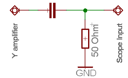
When doing this measurements, I realized a interesting fact. There are two different termination schemes used in scopes. The old Tektronics CSA 404 with an 11A34 amplifier module uses schematic 1 to achieve 50 Ohm input impedance. This yields a high pass cuttoff frequency of ~10 Hz. The second scope, a Tektronix TDS 3034 (which was used to make the screenshots), uses schematic 2, which yields in a high pass cuttoff frequency of ~200 kHz. This is not acceptabe for the step response measurements, so 1 MOhm input termination was used. This is OK when measuring the low frequency components of our step resonse (<10 MHz). When measuring high frequency switching noise (step 4), the 200kHz high-pass cutoff is no problem.
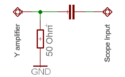
Schematic 2
50 Ohm Scope termination after coupling capacitor, yielding
in a high high-pass cutoff frequency
1st Step) FPGA not configured.
At this step we can measure the standby power consumption, which is mainly due to leakage. Notice that our scope also draws a lot of current when is uses schematic 1 for 50 ohm termination (50 Ohm at 2.5V = 50mA). We can also measure if our voltage regulator delivers the right voltages (can be seen as open cicuit voltage). We will write down the current consumption (80 mA) and core voltage (2.501 V). Note that this does not include current drawn by the 50 Ohm scope termination, since the scope used uses schematic 2 for 50 Ohm termination.
2nd Step) FPGA configured with empty design.
A simple design with a loop from an input to an output is loaded into the FPGA. After configuration, the power consumtion decreases, because the configuration logic inside the FPGA is disabled. The power consumtion of this minimal design is used as a calibration point for all other measurements. (40mA / 2.502 V)
3rd Step) FPGA configured but not toggling
Now power consumtion rises notably. From our first sight this is unexpexted, since nothing inside the FPGA changes its logic value (FlipFlops load always the same data). But this is not true, The clock network is running at full speed. So we can see that clock distribution power can be significiant. Thats why ultra low power technics use (clean) clock gating to reduce power consumption. But this has to be made in a safe way.
4th step) FPGA continous toggling
Now we start the firework! The power supply network is facing its worst nightmare. 1500 Flipflops toggeling simultaneously @147 MHz isnt peace of cake. Have a look at your Amp meter! The FPGA gets HOT quickly. But what can we see on the scope? Since the power consumption is constant, we can see high speed switching noise caused by insufficient decoupling capabilities of the ceramic caps. If you have a high-bandwidth scope (1 GHz+) and BAD power planes and high frequency decoupling caps, you might see the REALLY high frequency noise. With my 1GHz scope, I cant see this, most probably because the power planes and 10nF/100nF high frequency decoupling caps are doing a good job. With lower bandwidth sopes (100..300 MHz) you can only see the effect of the high speed decoupling caps. At this step we can also measure the voltage under full load. But make sure you measure the voltage seen by the FPGA, this means measure on the pins of the FPGA, not anywhere on the board!!! Because the power supply network has a limited resistance, which will cause a voltage drop from the voltage regulator output to the FPGA VCC pins. In a good design, this voltage drop should be less than 1% of the nominal voltage.
5th step) FPGA burst toggling
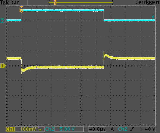
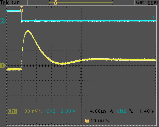
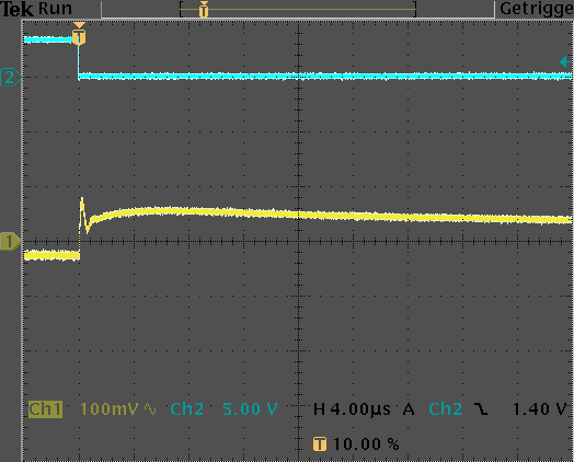
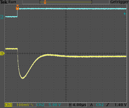
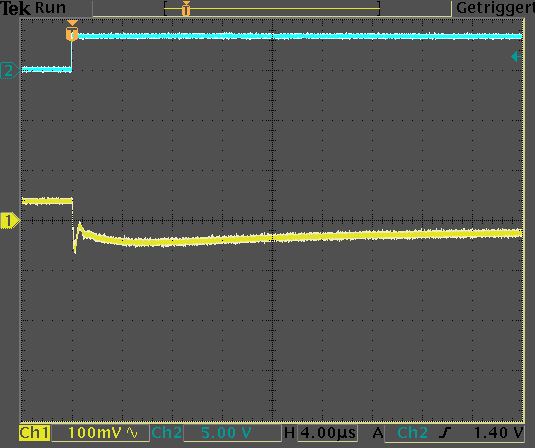
Finaly we reach the most interesting point. With the 16 bit counter, the toggeling of the FlipFlop array is a burst with a low frequency ON-OFF keying at 50% duty cycle, burst frequency is 1/65536 of the clock frequency, here ~2.2 kHz. This is the input step function noted above. And we see the reaction of the power supply network. If it would be perfect, we would see nothing but a straight line. But since this is not perfect world, we see overshot, ringing and a residual DC difference. The following pictures illustrate this (click to enlarge). The blue trace is the burst control signal from the 16 bit counter (MSB), the yellow trace the VCC core voltage.
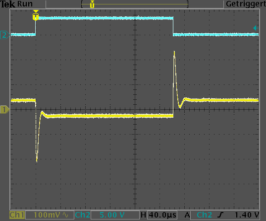
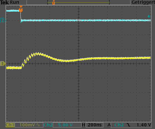
Magnification of turn off edge, with 10uF/110uF/110uF
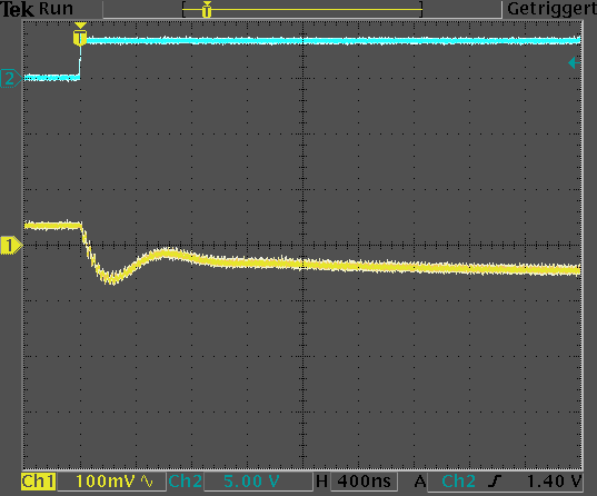
Magnification of turn on edge, with 10uF/110uF/110uF
What does this all mean?
First, the undershot when we change fron OFF to ON is caused
by insufficient middle frequency decoupling. The suddenly rising current
requirement can't be sourced by the middle frequency capacitor (too less
capacitance, so its delpeted soon), also not by the voltage regulator
(which is far too slow for this). The original demoboard has only a 10uF
tantalum type cap after the voltage regulator, which is far too less for
such a big load. Adding a 100uF in parallel reduces the undershoot significantly.
The overshot when we go from ON to OFF is similar to the undershoot,
but here the voltage regulator is too slow to switch from high output current
to low current. The not required current (charge) is stored in the middle
frequency capacitor, but since this is only 10uF the voltage rises fast.
To put it into easier words, its like to attempt to catch the rainwater
from a big roof with a small barrel, which will cause the water level in
the barrel to rise quickly.
What causes the DC-level shift? Now, this is the DC-resistance
of the power supply network from the output of the regulator (where it
senses the output voltage) to the VCC pin to the PLD. The current requirement
toggles between the current measured at step 3 (no toggling) and 4 (constant
toggling). From the scope we see ~70mV of voltage difference and about
912mA of current difference, which results in 76mOhm of resistance. The
conlusion here is, that the connection between the regulator sensing point
and the VCC pins should have low resistance. Power planes are best, but
also short, fat traces will work. There are also power regulators with extra
voltage sensing inputs, which can be used to compensate for voltage drops along
the power supply network.
| Measurement | FPGA content | Icc [mA] |
|
|
| Step 1 | Not configured | |||
| Step 2 | Configured, no design* | |||
| Step 3 | Configured, not toggling | |||
| Step 4 | Configured, constant toggling | |||
| Step 5 | Configured, burst toggling |
Conclusion
In this paper a simple but powerful method for measuring the frequency response of the power supply network of PLDs was presented. The measurement can be accomplished much easier and with more commonly available equipment under more realistic conditions than classic network analyzer approaches. It leaves a lot of room for experimentation with power supply decoupling in terms of capacitor placement and values.
Comments are very appreciated. Drop me a mail here.
Last change. 20.03.2007