Glitch Hunting
or
Why you should better respect the basic rules of synchronous design
Background
Nowadays, almost everything in our daily life contains electronic, and
almost everything contains digital electronics. This digital circuts have
to be designed by engineers.30 years ago, this task was accompished using
TTL standard logic. Complex functions filled dozens of boards each filled
with hundreds of ICs interconnected together. Later there were programmable
ICs (PAL & GALs) that could be user programmed and could do much more
complex (and problem optimized) functions in much less space (number of
ICs). Today, the most developed programmable logic ICs are FPGAs. They
are capable of data processing with clock rates of serval hundred MHz,
containing 10.000s of FlipFlops, Function generators and special features
(dedicated RAM, DLLs, special IO standards etc.)
The Problem
When designing digital system using FPGAs, some basic rules have to be
followed to get reliable results. In general, todays FPGAs (and their development
tools) are supposed to implement SYNCHRONOUS systems. But there are some
dirty asynchronous tricks that worked in the "good old days" of TTL systems,
because these "slow" ICs and their wireing in big boards acted as low pass
filters and coverd some bad effects. With modern FPGAs, which LUTs and FlipFlops
working with some hundreds of MHz, these nasty effects are NOT filtered
out, in fact these effects can (and WILL)
cause trouble. An expirienced designer will avoid such trouble,
but a beginner or someone who jumped right from the TTL age into nowadays
FPGAs lacks this experience (=suffered pain ?? ;-).
So we had such a case in our company and I would
like to share my expirience with the internet community.
Basics of glitches
The problem discussed here is glitching of signals. A glitch is a very
small pulse (just some nanoseconds long) on a signal caused by a decoder.
A decoder is in general a ROM which translates and input code (vector of
bits) into an output code. In FPGAs these decoders are formed by LUTs (Lookup
tables). Most FPGAs have 4 input LUTs which is simply a 16 bit ROM with
user defined content. When implementing decoders with more than 4 bit input
vectors, LUTs are cascaded to get the desired input bitwidth. In general,
the propagation delays of the individual input bits is not equal (no matter
if cascaded or simple decoder). So when more than one input bit is changing
simultaneously, some bits are "faster" than others. This can (and WILL)
cause the decoder output to jump from the actual output to some "inbetween"
output and back to the static output. When such an "glitchy" signal is used
as a clock or asynchronous reset signal, it will cause much trouble.
Have a look at the ciruit here.
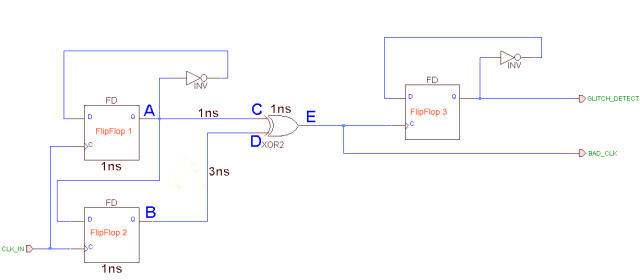
Circuit delays
This is a simple two bit shift register which actually only toggles between the two states
"01" and "10". Below the truth table for a XOR is shown.
| Input C |
Input D |
Output E |
| 0 |
0 |
0 |
| 0 |
1 |
1 |
| 1 |
0 |
1 |
| 1 |
1 |
0 |
Truth table of XOR
Looking at it in a static way, the output will always be '1'. But dynamicly this is not true.
Imagine the output of FlipFlop 1 (A) takes 1ns to reach the XOR input (C) and the output of FlipFlop 2 (B) takes 3 ns to the input of the XOR(D). Switching delay of
each FlipFlop (Clock to output) as well as combinatorical gate delay of the XOR is also 1ns. These are roughly real world values.
Lets look at the complete sequence when we transition from shift register state "10" to "01".

Timing diagram
- 0ns - Simulation start
- 1ns - clock input clk_in performes a rising edge, which will cause the FlipFlops to load new data
- 2ns - after a storage delay of 1ns new data is available at the output of the two FlipFlops (A and B); this happens very synchronous (+/- 100ps)
- 3ns - the new state of FipFlop 1 reaches the XOR (C) after 1ns of routing delay; the input to the XOR is now "11" which means a '0' at the output
- 4ns - the XOR output (E) transitions to '0' according to the input code of "11" after 1ns of gate delay
- 5ns - the second input of the XOR changes to '0', because the signal from (B) arrived at (D) after 3ns of routing delay
- 6ns - the XOR reacts to the new input code of "01" and switches to '1' after 1ns of gate delay
A good old TTL gate would'nt even blink an eye, but those nowaday FPGAs are DAMM fast. Not just the LUTs, also the FlipFlops can toggle like hell.
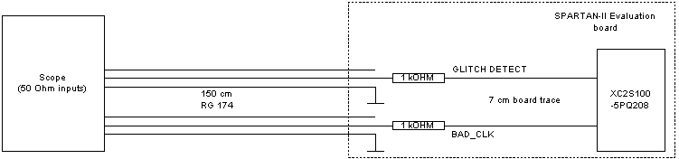
Measurement setup
These measurements where taken using the SPARTAN-II evaluation board from
Insight Electronics. It contains a XC2S100-5PQ208. The test circiut was clocked with 36 MHz (value not important, 1 MHz
would work too). The outputs under test where observed using high speed
attenuation probes suggested by the book
"High speed digital Design - A Handbook of Black Magic".
The risetime of such a probe is somewhere around
200ps. The scope used to take the screeshots had a bandwidth of 300 MHz,
additional measurements where taken using a 1 GHz scope (but no screenshot
could be taken, software problems). Note that the lines are not terminated. Reflections, overshoot and ringing are not important
for this tests.
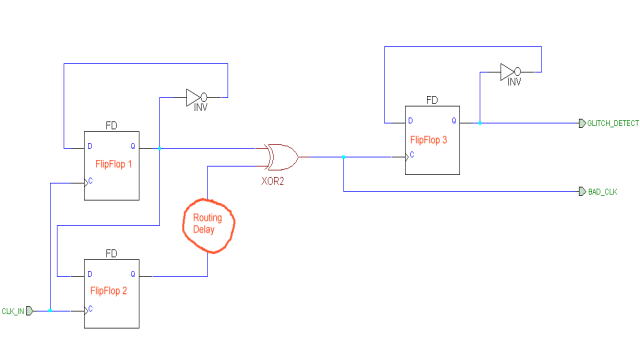
Experimental Setup
The test circiut was defined with VHDL.
It contains two FlipFlops which toggle with every clock cycle (simultaneously).
Since they are alway on complementary levels, the output of the XOR should
stay HIGH. But because of the unequal propagation delays of the two input
bit, the output of the XOR will glitch. This glitch will trigger a third
FlipFlop. The glitchy XOR output as well as the third FlipFlop output are routed
to output pins for observation.
Test circuit
The primitives where placed into special locations using constraints
to get deterministic results for different implementations. Also some IO cell
constraints are set to get maximum speed for the glitch output. In the
picture below you can see the logic grid of the XC2S100, which has a 20x30
CLB matrix.
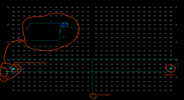
CLB Matrix
The delay between FF2 and the XOR was created by placing them far away
from each other. This distance was reduced step by step and the results
where documented in the screenshots.
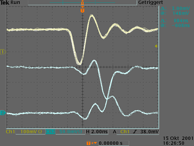
FlipFlop2 placed at column 30
This is the first attempt. Since the propagation delay difference is
long, so is the glitch. But have a close look, this is just a 1.5 ns pulse!!!
This is far from all specification (minimum pulse width) in the datasheet.
As you can see, FlipFlop 3 toggles on this glitch.
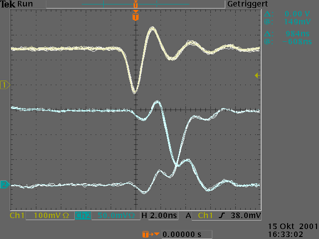
FlipFlop2 placed at column 15
Glitch is shorter but FlipFlop still toggles nice.
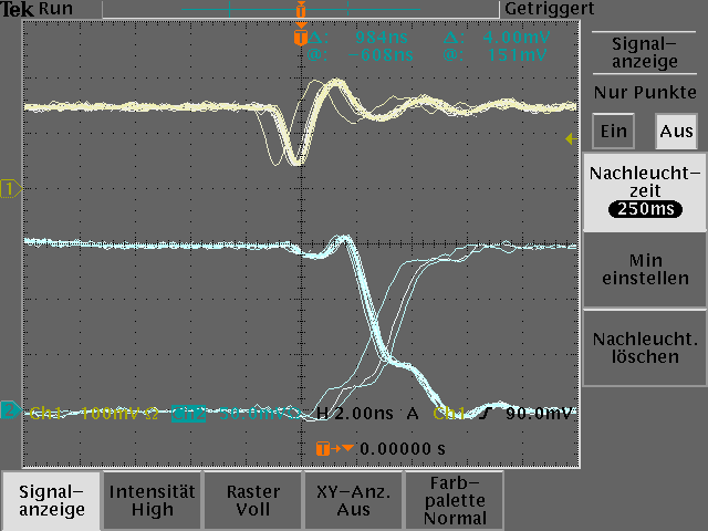
FlipFlop2 placed at column 10
Now its getting REALLY fast. We also see the limits of our scope, because
on the faster scope (1GHz) the glitch still touches down to zero volts. The FlipFlop
still toggles.
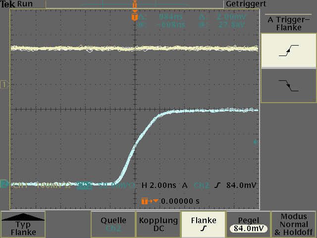
FlipFlop2 placed at column 8
FlipFlop still toggles, but we have clearly reached the limits of our
scope and the IO-cell. The glitch is no more visible outside (Also not
visible on the 1GHz scope). Since the IO-cell has to deliver up to 24 mA
and contains ESD protection circuitry, the structures (transistors, connections)
are much bigger (and so have more parasitic capacitance) which makes them
slower than the tiny structures inside the FPGA. We can also see that the
distortion on the glitch_detect output was caused by crosstalk from the
strong (24mA, FAST) bad_clk IO-cell.
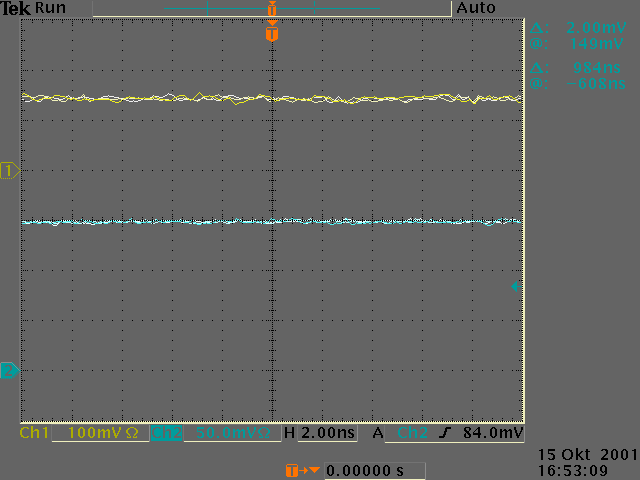
FlipFlop2 placed at column 3
Now we have reached the limit of our technology. The glitch is simply
too small to be "seen" by the FlipFlop 3. Only god know how the glitch
inside looks like. But be careful. This does not mean that you can get
a glitch free decoder by placing the FlipFlops driving the decoder this
close (or closer). The speed of the cells varies with temperature (hot
= slow, cold = fast), supply voltage (high = fast, low = slow) and part
to part variations. Don't count on the low speed of your technology to
act as a glitch filter! If you want to convert your design to a faster
technology (faster FPGA, FPGA to ASIC conversion) this design practice
WILL
fail!
The only reliable ways to avoid a glitch are
- change just one input at a time (gray code)
- use a FlipFlop at the decoder output to sample (register) the signal
If you have some comments, criticism or whatever, drop me a mail.
Last update: 20.03.2007


