GC_ET_AP.html
2021-07-18 11:47:32
2022-08-25 05:27:12
All-Pass Circuits
*** Results : Non-Resonant All-Pass stages can produce Notches usable in the Dual-Notch process.
*** Results : More stages are required, and Notches are not as deep as with AFX, but Very Deep Enough.


*** Working Circuits : (GC_ET_AP_Ckt_B.html) (click)
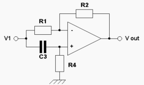
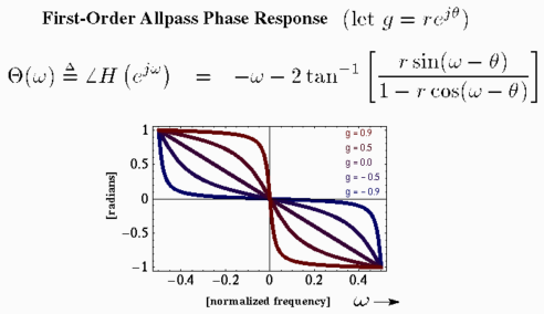
Developmental versions of All-Pass circuits
*******************************************************************************
Contributors to this project :
*******************************************************************************
Below: All Circuits require new Schem to match the Bode plots.
Freq are 7Hz and 700 Hz. Resistors need correction.
### Lo=7Hz (1M Ohm) Hi=700Hz (10 K Ohm).
.
*** Simple All-Pass Dual-Notch Circuit , Voltage-Mixer Final
******* Simple Developmental ckt , proof of concept.
***********************************************************************
### Below is the Revised and Simplified All-Pass Schematic
### One AP Lo-Pass combined with 12 AP Hi-Pass stages.
### Lo=7Hz (1M Ohm) Hi=700Hz (10 K Ohm).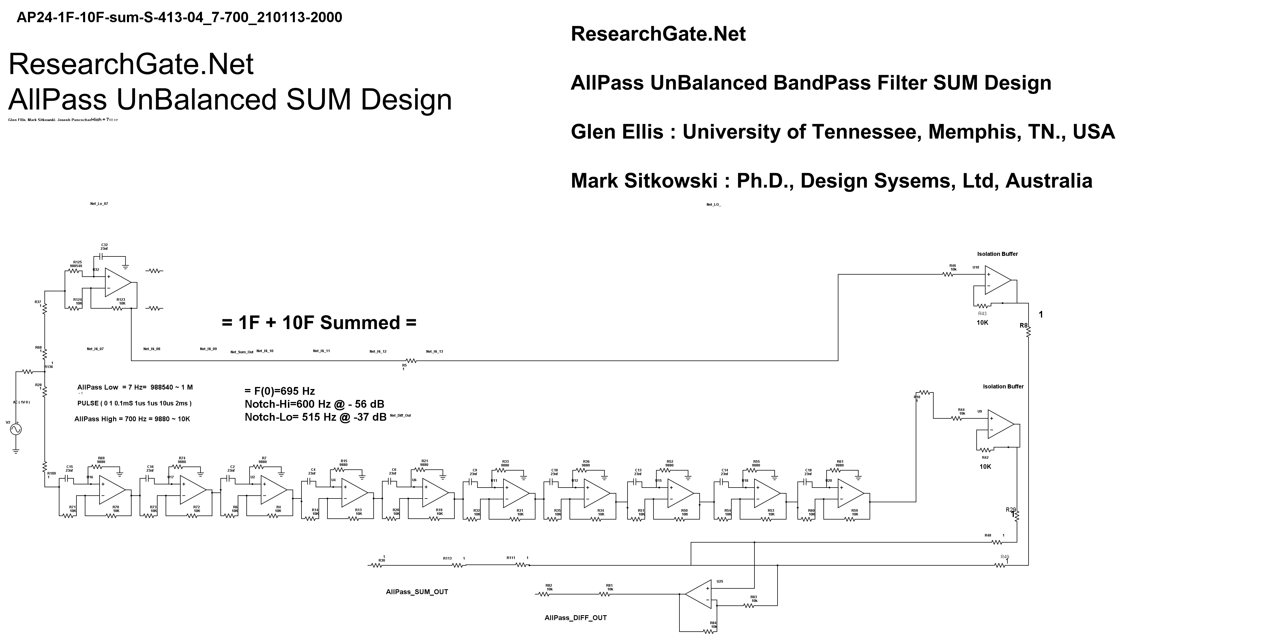
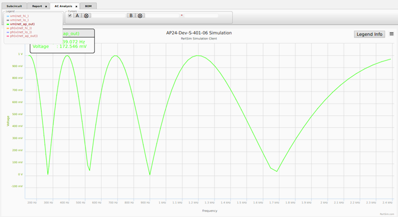
*** Below is the Revised All-Pass Bode Plot for All-Pass V(out)
*** showing Notches where "w=0" or "w=p" i.
*** The tick indicates f(700).
*** The two adjacent notches [ f(515) and f(900) ]
*** are exactly useful for building a Working Band-Pass Filter. 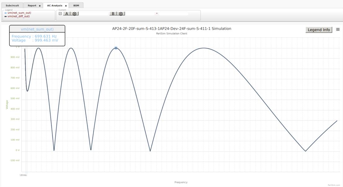
*************************************************************************************************************************************************
*************************************************************************************************************************************************
*************************************************************************************************************************************************
*** In this All-Pass project,
*** the authors accidentally tuned all the All-Pass-filter stages to f(0) = 7 Hz and f(0) = 700 Hz ,
*** which accentuates the "w" notches at each "0" and each "pi" point in the spectrum.
*** Observing the useful Bode plots, we explored further, along this Accidental Path.
*** In the fully developed #1 Working Circuit,
*** we preceeded and followed the All-Pass array
*** with Multi-FeedBack Band-Pass OpAmp Active Filters
*** to reduce unwanted side-band signals ( away from f(0) = 700 Hz ).
*** The authors explored the "UnBalanced" ( 700 Hz and 700 Hz ) approach.
*** The All-Pass-Lo is tuned to 692 Hz.
*** The All-Pass-Hi is tuned to 692 Hz.
*** These frequencies were chosen to utilize standard resistor values.
*** Presented above is a Simplified Proof-of-Concept All-Pass Filter
*** showing the array of notches,
*** two of which are +/- f(700) and exactly useful.
*********************************************************
*** Below are the Developmental All-Pass Circuits:
*** Right-Click Schematics and Plots for larger image ***
*****************************************************************
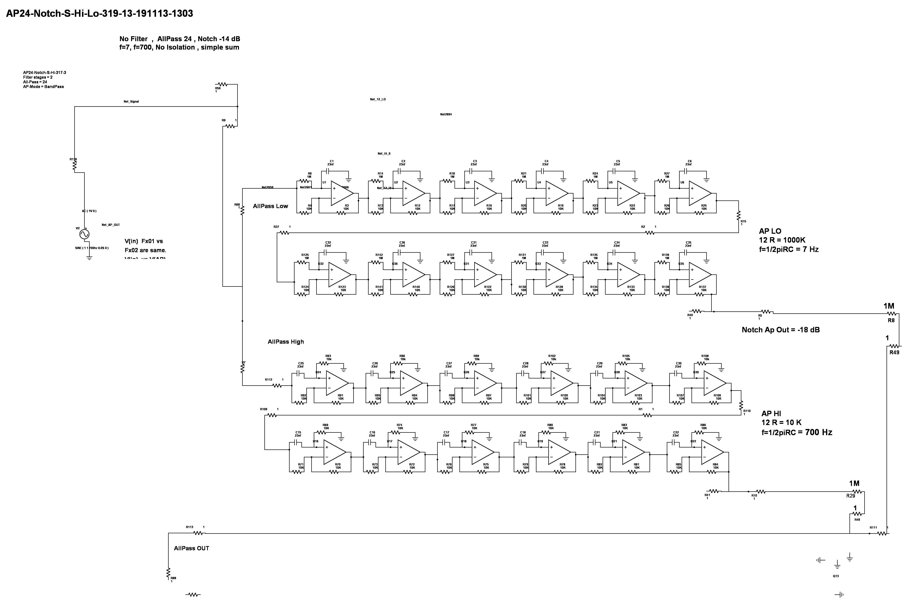 )
)### Below is the Original RAW All-Pass V(out) showing Notches where "w=0" or "w=pi" .
*** this observation lead to further experimental designs.
 )
)
*************************************************************************
*************************************************************************
*************************************************************************
*** Addendum **********************************************************
*************************************************************************
*** "No Notch" failed schematic :
....... Balanced Design LO=700 Hz / HI=700 Hz
....... combined by Voltage-Mixing .
*** This type of topology is frequently employed to produce audio phase shifting,
*** with each stage staggered at 1/10 f(0) to cover the entire audio spectrum.
*** Band-Pass aligned with w=0 and w=pi.
*** produces NO DUAL-NOTCHES .
*************************************************************************************************************************************************
*************************************************************************************************************************************************
*************************************************************************************************************************************************
*** In this #1 project,
*** the authors accidentally tuned all the All-Pass-filter stages to
f(0) = 7 Hz w 1M Ohm
(0) = 700 Hz w 10K Ohm
*** which
*** accentuates the "w" notches at each "0" point
*** accentuates each "pi" point
*
*** Observing the useful Bode plots, we explored further, along this accidental path.
*** In the fully developed #1 working circuit,
*** we preceeded and followed the All-Pass array
*** with Multi-FeedBack Band-Pass OpAmp filters
*** to reduce unwanted side-band signals ( away from f(0) = 700 Hz ).
*** The authors explored the "UnBalanced" ( 7 Hz and 700 Hz ) approach.
*** The All-Pass-Lo is tuned to 6.20 Hz.
*** The All-Pass-Hi is tuned to 692 Hz.
*** These frequencies were chosen to utilize standard resistor values.
*** Further #2 development will be done using the"UnBalanced" design
*** with f(0) at 650 Hz and 750 Hz to observe the effect.
*** DUAL-NOTCH Band-Pass schematic :
*** Un-Balanced design : LO=007 Hz and HI=700 Hz, Hi/Lo Voltge-Mixed ,
*** Band-Pass aligned with w=0 and w=pi.
*** DUAL-NOTCHES down to -50 dB .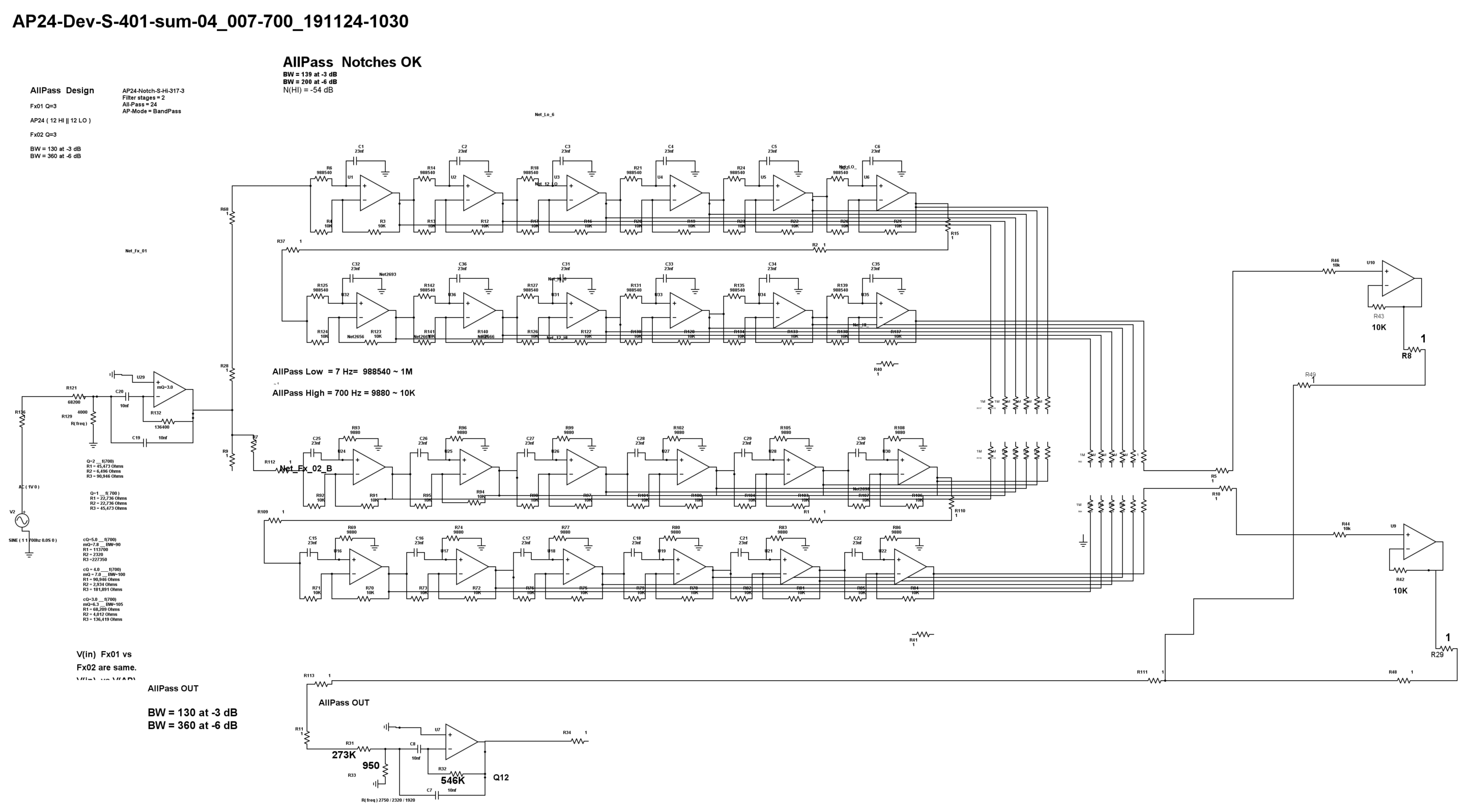
*** DUAL-NOTCH Bode Plot, Scale : 700mV = -3dB ; 500mV = -6dB.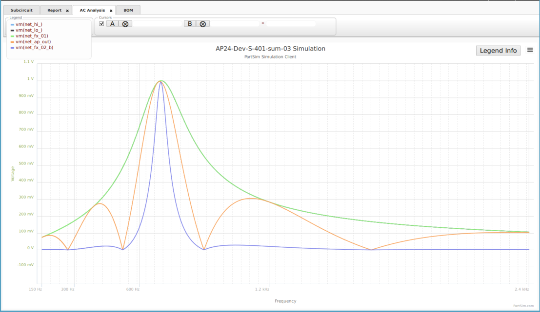
****************************************************************************************
****************************************************************************************
****************************************************************************************
*** No-Notch Failed schematic :
*** Un-Balanced LO=007 Hz and HI=700 Hz, Hi/Lo Differentiated
*** Band-Pass aligned with w=0 and w=pi.
*** NO Notches.
*** Differential method of combining the Hi/Lo signals does not produce a Dual-Notch effect.
*** Bode of NO-Notch ; Scale : 700mV = -3dB ; 500mV = -6dB
*********************************************************************
*********************************************************************
*********************************************************************