 Develop a process flow for fabricating 0.25 um CMOS for low temperature operation.
Determine design parameters necessary to achieve maximize performance and reliability at low temperatures.
Technical Approach:
 TCAD tools will be used to study the impact of certain process steps on device and circuit performance.
Using simulation results, device fabrication will be performed at the Stanford Nanofabrication Facility.
1996 Accomplishments:
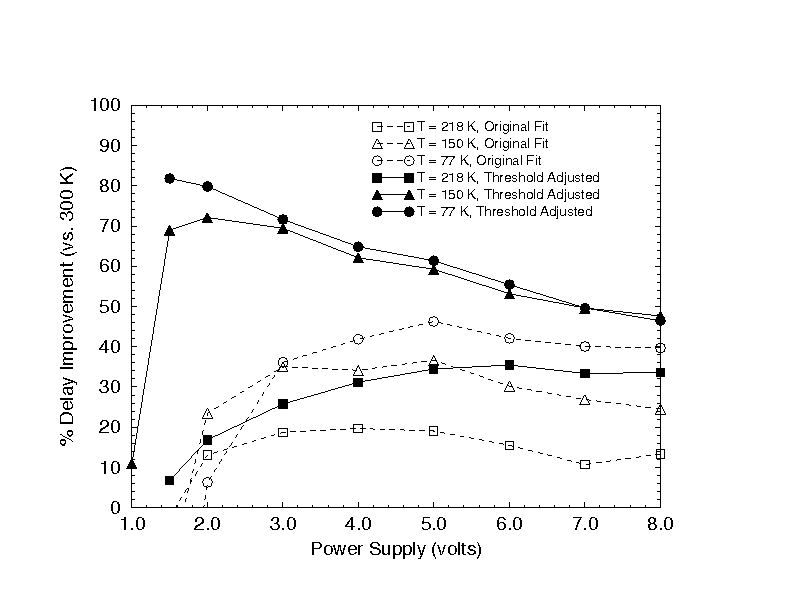
 Through careful and proper design, a 2-3x improvement in performance versus room temperature is possible. (see below)
Test chip mask has been designed and fabricated.
Thin gate oxide integrity (using both n+ and p+ poly gates) have been evaluated with good results.
First transistor run scheduled to start November 1996.
Bibliography:
"Process Modification for Improved Low Temperature CMOS Performance", Cliff Hwang, Ching Jenq, Bob Hammond, Jason Gillick, and Jason Woo, Workshop on Low Temperature Electronics II, Leuven, Belgium, June 26-28, 1996.
Questions or comments? Contact [email protected]
Last updated: 12/15/96
 Back to Cliff's Research Experience.
![]()
![]()