A STUDY ON SWIFT HEAVY ION
IRRADIATION INDUCED MODIFICATIONS IN Si, GaAs SURFACES and Pd /n-GaAs INTERFACE
ABSTRACT
of
Ph.D. Thesis
Submitted by
Om Prakash Sinha
Supervisor
Dr. P.C.
Srivastava
DEPARTMENT OF PHYSICS
BANARAS HINDU UNIVERSITY
Submitted
on : 31st Dec. 2001
Awarded on : 19th Feb.
2003
=======================================================
T
he effect of Swift heavy ion irradiation on electronic materials and devices is of significance both from fundamental as well as applied aspects. The swift heavy ion irradiation in electronic materials and devices has not been studied in detail and the related effects are yet to be fully understood. It has a direct relevance to simulate the degradation effects of electronic devices in space and in high radiation environment. The swift heavy ion in MeV range penetrates the semiconducting substrate quite deep in the bulk and hence a deep buried implantation layer can be worked out by swift heavy ion irradiation. Moreover, the swift heavy ion loses most of their energy through electronic energy loss on the surface of the target to result unique surface modifications.
Semiconductor surfaces (silicon and gallium arsenide) and Metal /Semiconductor devices on gallium arsenide has been studied from various techniques after swift (~100 MeV) heavy ion (Si7+ & Au7+) irradiation. For surface morphological studies, AFM has been used. Electronic flow characterization (I-V & C-V) studies for defects states characterization has been done. Moreover, the hydrogen passivation of the irradiated devices has been studied to investigate the hydrogen healing effects of irradiation induced damage effects. XPS studies have been carried out to study the chemical changes and elemental analysis at the device interface after the irradiation. SEM with EDAX has also been performed for the quantitative elemental analysis of the irradiated surfaces.
Chapter – I of the present thesis describes the general introduction of the irradiation and its related phenomena. The present thesis is mainly concerned with Swift Heavy Ion irradiation induced modifications in semiconductors (Si & GaAs). Therefore, the different energy loss processes, irradiation effects in solid and irradiation-induced defects are dealt with in relatively greater details. Moreover, the review of existing literature on Swift Heavy Ion irradiation has been carried out.
Chapter – II describes an overview of the techniques used for the irradiation and the surface morphological studies. The details of the ‘Pelletron Machine used for the irradiation and of the ‘Atomic Force Microscope’ used for surface morphological studies have been described.
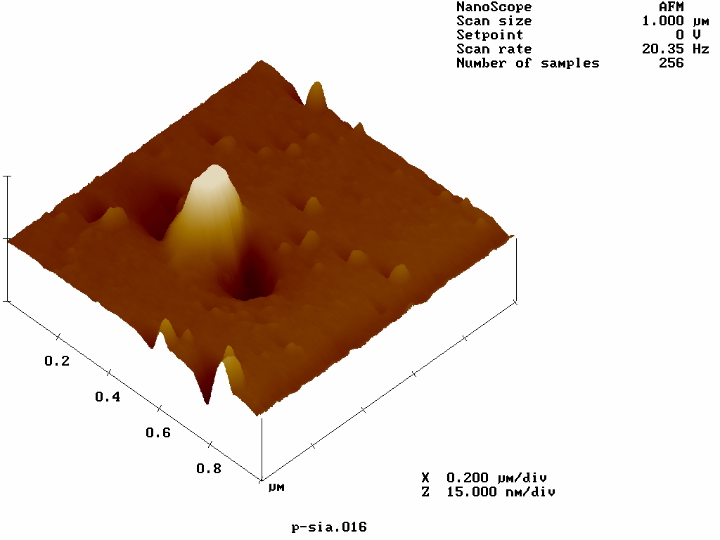
Chapter – III describes the experimental results of surface morphological studies by AFM of n-Si & p-Si and n-GaAs. The swift heavy ion (of Au7+) irradiation induced modification shows the formation of craters and hills, which are flanking to each other. For the few cases, the hill is flanking by craters from the either side and such observation has been made by us for the first time. Moreover, the p-type silicon shows more radiation hardness than the n-silicon. In gallium arsenide, linear arrangement of hillocks along the crystal plane has been observed. The lighter ion (of Si7+) irradiation shows the clear evidence of melting and regrowth phenomena for p-silicon. It is also found that the damage zones are distributed on the surface of silicon whereas it is localized for GaAs substrates. The quantitative estimate of the features revealed that the volumes of craters are greater (by a factor of 2 to 5) than the volume of the hill. The difference in number of missing silicon atoms from craters region and number of piled up silicon atoms in hill region indicate that the density of hill is higher than the craters and a fraction of atoms from the craters region has sputtered out due to a violent expulsion of atoms caused by electronic stopping.
Chapter – IV deals with the experimental results of electronic
flow characterization of swift heavy ion irradiated Pd/n-GaAs interface.
It also describes the basic concepts of “Metal-Semiconductor Contact”. The
Current-Voltage and Capacitance-Voltage studies (at different frequencies)
for before irradiation, after irradiation and after irradiation & hydrogenation
have been carried out. The hydrogenation studies have been carried out to
study the effect of hydrogen on irradiated devices. The realised diodes
(metallization after irradiation) show improvement of characteristics after
the hydrogenation. The devices after the irradiation to the higher fluence
show a heavily damaged surface due to swift heavy ion irradiation. The fabricated
diodes( metallization before the irradiation) also show a poor diode characteristics
after the irradiation with no significant effect of the hydrogenation on
these devices.
The Capacitance –Voltage studies of
these devices show the change of conductivity type from n-to p-type after
the irradiation. The C-V characteristics of the fabricated devices after the
irradiation and hydrogenation show the presence of a peak near zero bias which
has been identified as acceptor states at Ev = 0.75eV of ~5x10
7cm-2. The observed state has been assigned to As vacancies.
The results have shown the presence of radiation-induced defects which cause carrier removal and compensation to cause the observed high resistivity and conductivity type change in the post irradiated devices. The possibility of amphoteric Si doping atoms, which are changing their sites from Ga to As to cause the conductivity type change from n- to p-type has been invoked.
Chapter – V describes the experimental details and results of X-ray Photoelectron Spectroscopic studies of swift heavy ion irradiated Pd/n-GaAs surface/interface. The XPS studies show the As deficient surfaces which becomes more deficient after the irradiation. Moreover, SEM with EDAX studies also supports the observation of As deficient surfaces for the irradiated n-GaAs surface/interface.
Finally in Chapter –VI, all the results of the present thesis has been summerized.
![]()
