
At present, small molecule?based prototype displays look better--they have more colors--than polymer versions, but PLED proponents are confident about closing the gap.
| Leia o texto abaixo do PHD em física pela Harvard, Webster E. Howard, com auxílio do dicionário no computador (para economizar tempo). Atente, principalmente, para os graus dos adjetivos. | ||||||||||||||||||
| Prévia do texto: o artigo abaixo foi retirado de uma das mais conceituadas revistas de ciência do mundo: a Scientific American. Trata-se de uma nova tecnologia de projeção de imagens por meio de filmes orgânicos. Dessa forma literalmente será possível "vestir" uma tela de televisão. Bons estudos. | ||||||||||||||||||
| Scientific American ? Feb 2004 | ||||||||||||||||||
| Better Displays with Organic Films | ||||||||||||||||||
|
||||||||||||||||||
| Light-emitting organic materials offer brighter and more efficient displays than LEDs. And you'll be able to unroll them across a tabletop | ||||||||||||||||||
| By Webster E. Howard | ||||||||||||||||||
| Before the videocassette recorder there was the movie projector and screen. Perhaps you remember your fifth-grade teacher pulling down a screen--or dad hanging a sheet on the wall, ready to show visiting friends the enthralling account of your summer vacation at the shore. Just as the film got started, the projector bulb often blew out. | ||||||||||||||||||
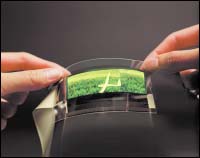
| Those days did have one advantage, though: the screen was light, paper-thin and could be rolled into a portable tube. Compare that with bulky television and computer screens, and the projector screen invokes more than just nostalgia. Could yesterday's convenience be married to today's technology? | ||||||||||||||||||
| The answer is yes, thanks to organic light-emitting materials that promise to make electronic viewing more convenient and ubiquitous. Used in displays, the organic materials are brighter, consume less energy and are easier to manufacture (thus potentially cheaper) than current options based on liquid crystals. Because organic light-emitting diodes (OLEDs) emit light, they consume significantly less power, especially in small sizes, than common liquid-crystal displays (LCDs), which require backlighting. OLEDs also offer several exciting advantages over common LEDs: the materials do not need to be crystalline (that is, composed of a precisely repeating pattern of planes of atoms), so they are easier to make; they are applied in thin layers for a slimmer profile; and different materials (for different colors) can be patterned on a given substrate to make high-resolution images. The substrates may be inexpensive glass or flexible plastic or even metal foil. | ||||||||||||||||||
| In the coming years, large-screen televisions and computer monitors could roll up for storage. A soldier might unfurl a sheet of plastic showing a real-time situation map. Smaller displays could be wrapped around a person's forearm or incorporated into clothing. Used in lighting fixtures, the panels could curl around an architectural column or lie almost wallpaperlike against a wall or ceiling. | ||||||||||||||||||
| LEDs currently have longer lifetimes than organic emitters, and it will be tough to beat the widespread LED for use in indicator lamps. But OLEDs are already demonstrating their potential for displays. Their screens put out more than 100 candelas per square meter (about the luminance of a notebook screen) and last tens of thousands of hours (several years of regular use) before they dim to half their original radiance. | ||||||||||||||||||
| Close to 100 companies are developing applications for the technology, focusing on small, low-power displays [see illustration right]. Initial products include a nonflexible 2.2-inch (diagonal) display for digital cameras and cellular phones made jointly by Kodak and Sanyo, introduced in 2002, and a 15-inch prototype computer monitor produced by the same collaborative venture. The global market for organic display devices was about $219 million in 2003 and is projected to jump to $3.1 billion by 2009, according to Kimberly Allen of iSuppli/Stanford Resources, a market-research firm specializing in displays. | ||||||||||||||||||
| What LED to OLED | ||||||||||||||||||
| Crystalline semiconductors--the forerunners of OLEDs--trace their roots back to the development of the transistor in 1947, and visible-light LEDs were invented in 1962 by Nick Holonyak, Jr. They were first used commercially as tiny sources of red light in calculators and watches and soon after also appeared as durable indicator lights of red, green or yellow. (When suitably constructed, LEDs form lasers, which have spawned the optical-fiber revolution, as well as optical data storage on compact discs and digital video discs.) Since the advent of the blue LED in the 1990s [see "Blue Chip," by Glenn Zorpette; Scientific American, August 2000], full-color, large-screen television displays made from hundreds of thousands of LED chips have appeared in spectacular fashion on skyscrapers and in arenas [see "In Pursuit of the Ultimate Lamp," by M. George Crawford, Nick Holonyak, Jr., and Frederick A. Kish, Jr.; Scientific American, February 2001]. Yet the smaller sizes used in devices such as PDAs (personal digital assistants) and laptops are not as practical. | ||||||||||||||||||
| LEDs and OLEDs are made from layers of semiconductors--materials whose electrical performance is midway between an excellent conductor such as copper and an insulator such as rubber. Semiconducting materials, such as silicon, have a small energy gap between electrons that are bound and those that are free to move around and conduct electricity. Given sufficient energy in the form of an applied voltage, electrons can "jump" the gap and begin moving, constituting an electrical charge. A semiconductor can be made conductive by doping it; if the atoms added to a layer have a smaller number of electrons than the atoms they replace, electrons have effectively been removed, leaving positively charged "holes" and making the material "p-type." Alternatively, a layer that is doped so that it has an excess of negatively charged electrons becomes "n-type" [see illustration below]. When an electron is added to a p-type material, it may encounter a hole and drop into the lower band, giving up an amount of energy (equal to the energy gap) as a photon of light. The wavelength depends on the energy gap of the emitting material. | ||||||||||||||||||
| For the production of visible light, organic materials should have an energy gap between their lower and higher conduction bands in a relatively small range, about two to three electron volts. (One electron volt is defined as the kinetic energy gained by an electron when it is accelerated by a potential difference of one volt. A photon with one electron volt of energy corresponds to the infrared wavelength of 1,240 nanometers, and a photon of two electron volts has a wavelength half as much--620 nanometers--a reddish color.) | ||||||||||||||||||
|
||||||||||||||||||
| A Surprising Glow | ||||||||||||||||||
| Organic semiconductors are formed as aggregates of molecules that are, in the technologies being pursued, amorphous--a solid material, but one that is noncrystalline and without a definite order. There are two general types of organic light emitters, distinguished by "small" and "large" molecule sizes. The first practical p-n-type organic LED, based on small molecules, was invented in 1987 by Ching W. Tang and Steven A. Van Slyke of Eastman Kodak, after Tang noticed a surprising green glow coming from an organic solar cell he was working on. The duo recognized that by using two organic materials, one a good conductor of holes and the other a good conductor of electrons, they could ensure that photon emission would take place near the contact area, or junction, of the two materials, as in a crystalline LED. They also needed a material that held its electrons tightly, meaning that it would be easy to inject holes. For the light to escape, one of the contacts must be transparent, and the scientists benefited from the fortunate fact that the most widely used transparent conducting material, indium tin oxide, bound its electrons suitably for p-type contact material. | ||||||||||||||||||
| The structure they came up with has not changed much over the years and is often called "Kodak-type," because Kodak had the basic patent [see sidebar]. Beginning with a glass substrate, different materials are deposited layer by layer. This process is accomplished by evaporating the constituent materials and letting them condense on the substrate. The total thickness of the organic layers is only 100 to 150 nanometers, much thinner than that of a conventional LED (which is at least microns in thickness) and less than 1 percent of the thickness of a human hair. Because the molecules of the materials used are relatively lightweight--even lighter than a small protein--the Kodak-type OLEDs are referred to as "small molecule" OLEDs. | ||||||||||||||||||
| After their initial insight, Tang and Van Slyke tinkered with the design to increase efficiency. They added a small amount of the fluorescent dye coumarin to the emitter material tris (8-hydroxyquinoline) aluminum. The energy released by the recombination of holes and electrons was transferred to the dye, which emitted light with greatly increased efficiency. Deposition of additional thin layers of indium tin oxide and other compounds next to the electrodes altered the interaction of the thicker layers and also improved the efficiency of the injection of holes and electrons, thereby further upping the overall power efficiency of the fluorescent OLED. | ||||||||||||||||||
| Organic LEDs of this small-molecule type are used to make red, green and blue light, with green light having the highest efficiency. Such green-emitting OLEDs can exhibit luminous efficiencies of 10 to 15 candelas per ampere--about as efficient as commercial LEDs today--and seven to 10 lumens per watt, values that are comparable to those for common incandescent lamps. | ||||||||||||||||||
| Spin the Puddle | ||||||||||||||||||
| The second type of organic light emitter is the large-molecule light-emitting polymer, also known as the polymer light-emitting diode (PLED). Reported in 1990 by Jeremy Burroughes and his colleagues at the University of Cambridge, this device incorporates polymers--made from unions, often chains, of smaller organic molecules--to form the layers. Polymer LEDs are formed by spin coating: applying a thin layer of polymer to a flat substrate and then spinning the substrate at a high speed (typically 1,200 to 1,500 revolutions per minute) to spread the polymer puddle by centrifugal force. The spin coating is followed by a baking step to remove the solvent and, in some cases, to complete the polymerization. This film formation process is generally more economical than the thermal evaporation method discussed above. Polymers have had an edge over Kodak-type small-molecule devices in power efficiencies because the greater electronic conductivity of the polymer layers allows lower operating voltages. | ||||||||||||||||||
| The original PLED consisted of a single active layer of a polymer called polyphenylene vinylene (PPV) between dissimilar metal contacts such as indium tin oxide and calcium, as in an OLED, to provide injection of both holes and electrons. Indium tin oxide is a metal that tends to inject holes, and calcium is a metal that tends to inject electrons. Current PLEDs use a second polymer layer for hole injection and transport. The polymer PPV produces yellow light, with an excellent efficiency and lifetime; at computer-monitor luminance levels, such a PLED can last more than 10,000 hours--about 10 years of regular use. (Full color has been demonstrated, but the only commercial product to date uses yellow.) Other polymers and mixed polymers (two different polymers in solution) have been developed, notably by Dow Chemical, based on the organic molecule polyfluorene. These configurations can be modified to produce a full range of colors, from red to green, by varying the lengths of the segments of the co-polymers. Unfortunately, the display lifetimes of these colors have not been comparable to that of PPV, and blue is not yet ready for prime time. | ||||||||||||||||||
| Overcoming Limitations | ||||||||||||||||||
| Although today's fluorescent OLEDs and PLEDs are fairly energy-conserving, there is room for improvement. One limiting factor of the first-generation devices is electron spin, an intrinsic quantum property that determines how the particles react to a magnetic field. When an electron and a hole come together, they form an entity known as an exciton. The quantum-mechanical rules of interaction of the electron and hole spins dictate that for most materials only one in four excitons formed will be able to give up its energy as a photon, whereas the others will lose their energy as heat. | ||||||||||||||||||
| This problem was overcome in 1998 by a team led by Stephen R. Forrest of Princeton University and Mark E. Thompson of the University of Southern California. They developed OLED devices in which the emitting material contained a heavy metal such as platinum or iridium. In a heavy metal atom the outer electrons are, on average, far from the nucleus, and consequently have a large angular momentum of rotation. This momentum interacts with the spin of other electrons, essentially creating conditions where all the excitons can emit light rather than heat, raising the theoretical efficiency to nearly 100 percent. These new emitters are referred to as phosphorescent OLEDs, to distinguish them from the more common fluorescent OLEDs. | ||||||||||||||||||
| The phosphorescent small-molecule OLEDs generate impressive efficiency gains without any significant loss of lifetime, except for the case of blue emitters. No good blue-emitting phosphorescent material yet exists, although major efforts are under way at numerous laboratories to remedy this situation. | ||||||||||||||||||
| Is there a way to pair the many colors produced by small-molecule OLEDs with the economic benefits of the spin solution coating used in PLEDs? One recent exciting development builds on the successful application of these phosphorescent materials to potentially do just that. Workers at the University of Oxford, the University of St. Andrews and OpSys in Oxford, England, have synthesized molecules known as dendrimers that may prove to combine the desirable aspects of small molecules and polymers. In a dendrimer, a phosphorescent molecule serves as the core around which layers of branching ring structures are bonded, forming a large molecular ball. If the branching elements are suitably chosen, these molecules can be dissolved, and films can be formed by spin coating and baking, as with polymer materials. Already dendrimer devices have yielded very high luminous efficiencies (more than 50 candelas per ampere and 40 lumens per watt). | ||||||||||||||||||
| Organic light emitters achieve the same image quality as bulky cathode-ray tubes (CRTs) and LCDs, although the manufacturing process differs. For good perceived image quality, the red, green and blue pixel-producing groups, called triads, must be more densely spaced than 100 per inch (or roughly 40 per centimeter) so that the eye can merge the colors without noticing the underlying image structure. Both CRTs and LCDs achieve such precision with photolithography, in which a projected light image creates a pattern for laying out a material design. Each phosphor or color-filter material is suspended in a photosensitive resin matrix and spread over the entire display area. Wherever light hits the material, the matrix is rendered insoluble and the rest of the material is then dissolved, or developed, away. Three successive applications, one for each color, complete the process. | ||||||||||||||||||
| In contrast, small-molecule color OLEDs are patterned by evaporating the emitter materials through a shadow mask. The mask is displaced slightly for the successive evaporations of the red-, green- and blue-producing materials and can be manipulated with a 10-micron accuracy, for 250-micron triad dimensions. The preferred application method for full-color PLEDs is ink-jet printing, a technique widely used in PC color printers. High-precision versions of printers with polymer inks can pattern the red, green and blue polymer emitters with a precision of five to 10 microns. | ||||||||||||||||||
| Products Today and Tomorrow At present, small molecule?based prototype displays look better--they have more colors--than polymer versions, but PLED proponents are confident about closing the gap. |
||||||||||||||||||
| Color OLEDs and PLEDs can also be made by using a white light emitter and tiny color filters, as is done with LEDs. This approach has been used by eMagin Corporation (the author's former organization) in Hopewell Junction, N.Y., to provide 800-by-600-pixel resolution in a 0.6-inch (diagonal) color microdisplay, built on a silicon microchip active matrix. Such displays are used, with magnifying optics, in helmets for pilots, soldiers and firefighters, as well as in headsets for applications such as three-dimensional PC games--an example of an innovative product made possible by the new organic emitter technology. | ||||||||||||||||||
| The military and others are also investigating technologies to make flexible organic light emitters. The U.S. Army Research Laboratory recently awarded $2 million to Universal Display Corporation in Ewing, N.J., to develop such an OLED display, which could be unrolled from a pen-size communications device. The Defense Advanced Research Projects Agency has also funded work on the flexible devices for battlefield displays. | ||||||||||||||||||
| Less dramatically, one can expect consistent and rapid progress in organic emitter and transport materials, as the number of interested companies and dedicated scientists grows. Already it has become clear that organic emitters offer almost unlimited opportunity for molecular engineering and synthesis to improve energy efficiency, product life and manufacturing cost. | ||||||||||||||||||
|
|
||||||||||||||||||
| WEBSTER E. HOWARD received a Ph.D. in physics from Harvard University in 1962 and spent his early years in semiconductor physics research. Since 1974 he has worked on various display technologies at IBM Research, ATT/Lucent and eMagin Corporation. His major efforts were in thin-film transistors and liquid-crystal displays. Most recently, as chief technology officer of eMagin, he led the development of OLED-based microdisplays for use in helmets and headsets. In 2003 he was awarded the Jan Rajchman Prize of the Society for Information Display for his contributions to flat-panel display technology. He is currently enjoying retirement, with more time for family, woodworking and golf. | ||||||||||||||||||