You can prepare your own PCBs at your home!...
STEP : 1
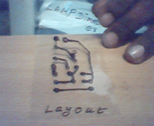
The first step in PCB design is preparation of PCB layout . There are lot of free softwares like DipTrace, Pspice and many more are available in the internet from which you can design your own PCB layout . Don't worry if you do not have such softwares, here i have an alternative method . Take a piece of OHP SHEET similar to the size of the copper plated board and trace the image of the layout by placing the OHP sheet over the layout model or simply draw the layout on the OHP/ white paper .
STEP : 2
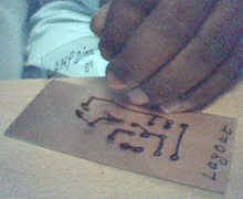
Place the OHP piece over the copper plated board and tie them together by means of cello tape . Now punch the board by a pin over the places in which holes have to be made ( this step is simply to mark the points on the board in which holes have to be drilled later).
STEP : 3
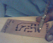
Now remove the OHP layout from the board and draw the layout on the board by taking the marked points as reference .
NextPages
![]()
![]()
![]()
![]()
![]() .
.
1 2
4
5
.
.
1 2
4
5