
|
Remote Sensing and Control System (Graduation Project -2001) |
6- Circuit Functioning
Simple devices were used for this project such as counters, pulse generators, logical gates, decoder and digital multiplexers. All these electronic devices would function at their specific time and are controlled through logical gates.
Pulse Generator: A pulse generator circuit is shown below. Its commonly known as IC555. We have to choose resistances Ra, Rb and Capacitance values. These will determine the frequency or timed pulses. f = 1.44 / [ C ( Ra + Rb )]
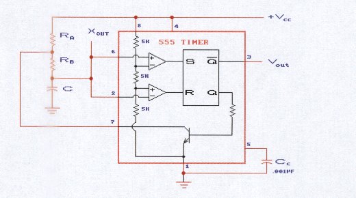
Figure 7.1
Time Control Circuits: Mostly these consists of logical gats and binary counter. The main function is to switch on a device for specific time t1 and then after it completes its function, to switch on another circuit for a specific time interval t2. The following circuit will introduce a delay with 1Hz timer clock as shown below: Let us omit the first bit, (considering "1" as high pulse and "0" Low pulse)
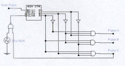
Figure 7.2
| Time | Binary counter | Pulse A | Pulse B | Pulse C |
| 1sec | 0000 | 0 | 0 | 0 |
| 2sec | 0001 | 0 | 0 | 0 |
| 3sec | 0010 | 1 | 0 | 0 |
| 4sec | 0011 | 1 | 0 | 0 |
| 5sec | 0100 | 0 | 0 | 0 |
| 6sec | 0101 | 0 | 0 | 0 |
| 7sec | 0110 | 0 | 0 | 0 |
| 8sec | 0111 | 0 | 0 | 0 |
| 9sec | 1000 | 0 | 1 | 0 |
| 10sec | 1001 | 0 | 1 | 0 |
| 11sec | 1010 | 0 | 0 | 0 |
| 12sec | 1011 | 0 | 0 | 0 |
| 13sec | 1100 | 0 | 0 | 1 |
| 14sec | 1101 | 0 | 0 | 1 |
From the table its clear that pulse at A, B and C are of duration 2sec each. The pulse A occurs after 2 sec. of the start and pulse B after 4 sec. from pulse A and C occurs after 2 sec. of pulse B. At 1101 the counter stops and needs a reset through a pulse to start the similar process agian. This could be shown in the graph below
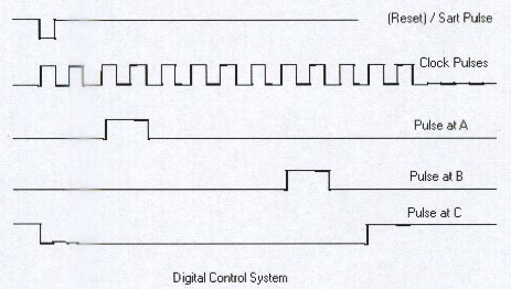
Figure 7.3
In this project Pulse A is connected to ADC enable, which finishes its function in 0.2sec and then Pulse B is connected to 8-bit parallel register which stores the value from the ADC. The Pulse C is tells the computer that data is ready. (Pin#12)
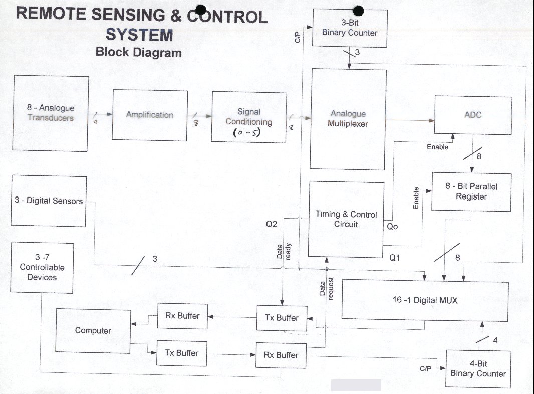
Parallel to Serial Conversion: Apart from 8-bit of data we need to transmit other information to the computer. This will make our data long and therefore over a long distances we have to transmit data serially to the computer. 8 bit data from parallel register, 3 bit data from sensor address, 3 bit data from digital sensors and 2 bits for start and stop = 16 bit of data to be transmitted. Therefore we need to use 16-1 digital MUX having 4 selectors connected to the 4-bit counter and pulsed through computer PP Pin#2. The output of the MUX goes to the computer PP Pin#10. The Block diagram could be explained as:
|
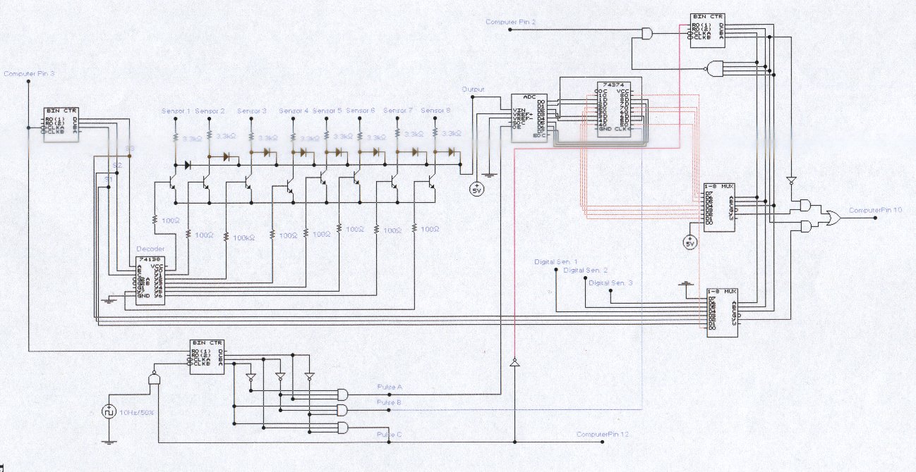
Complete Circuit Schematic |
Block Diagram |