Epitaxial Fe3Si fims stabilized on GaAs(113)A substrates Epitaxial Fe_{3}Si films stabilized on GaAs(113)A substrates
Epitaxial Fe3Si films stabilized on GaAs(113)A substrates
P. K. Muduli , J. Herfort , H.-P. Schönherr, K. H. Ploog
Paul-Drude-Institut für Festkörperelektronik,
Hausvogteiplatz 5-7, D-10117 Berlin, Germany
Aug 15, 2005
Abstract
We report epitaxial growth of the Heusler alloy Fe3Si on
high-index GaAs(113)A substrates by molecular-beam epitaxy. The
growth temperature and growth rate are optimized to 250 °C
and 0.13 nm/min, respectively for producing Fe3Si films with
structural properties comparable to that of Fe3Si films on
GaAs(001). The layers grown under these conditions exhibit high
crystal quality with smoother interface/surface and maintain the
(113) orientation of the GaAs substrate. The Fe-Si alloy
composition is varied around the Fe3Si stoichiometry using
these optimized growth conditions. The magnetic properties of a
typical Fe3Si layer with the best structural properties
exhibit a four-fold magnetic anisotropy, as expected from the
magnetocrystalline anisotropy.
A3.Molecular beam epitaxy A1.High resolution X-ray
diffraction B2.Magnetic materials B2.Fe3Si B2.GaAs(113)A
81.15.Hi Bb -i
Ferromagnet-semiconductor hybrid structures (FM/SC) are important
for the field of spintronics [1]. Elemental
ferromagnets like Fe, Co, Ni or their alloys which are usually
employed for such applications tend to react at the FM/SC
interface. Relative low growth temperatures are required to
suppress these interfacial reactions, which are considered to be
detrimental to spin dependent transport across the interface.
Alternative materials of better thermal stability and improved
interface quality are highly desirable for such applications. In
a previous work, [2] we reported the growth of
Fe3Si films on GaAs(001). Fe3Si has a cubic D03
crystal structure with a lattice constant very close to GaAs and a
high Curie temperature of 840 K [3]. Fe3Si
can also be regarded as a Heusler alloy Fe2FeSi as there are
two distinct crystallographic and magnetic Fe sites. In
ref [2], an optimum growth temperature range of
150 °C < TG < 250 °Cwas established, where
ferromagnetic films of high crystal and interface quality were
obtained [2]. This temperature is much higher
than usually used for the growth of Fe films on
GaAs [4,5,6]. Moreover, we have
recently demonstrated that the Fe3Si films are thermally
stable to ex-situ annealing at least up to
400 °C [7]. These properties make
Fe3Si, a very good alternative to elemental ferromagnets.
So far the growth of ferromagnets on GaAs substrates has been
focused mainly on the low-index surfaces. Much less work is
devoted to study ferromagnetic films on high-index semiconductor
surfaces. In fact, obtaining a stable high-index surface of a
ferromagnet in general is rather difficult. For instance, Fe films
deposited on Cu(113) did not maintain the same orientation
relationship with the substrate, which led to a highly strained
and distorted bcc Fe arrangement with (112)
orientation [8]. On the other hand, the thermal
stability and the ordering of such surfaces with reduced symmetry
and coordination number offer a variety of opportunities for
inducing new phenomena and are thus promising for new device
applications of the FM/SC [11]. The GaAs(113)A
surface in particular is characterized by a low surface symmetry
with the two major in-plane axes, namely [33[`2]] and
[[`1]10] being crystallographically in-equivalent.
Moreover, due to this reduced symmetry, we previously observed new
features in the planar Hall effect of Fe films on GaAs(113)A,
which cannot be understood in the usual picture of anisotropic
magnetoresistance [9,10]. In
this report we will demonstrate for the first time that a
ferromagnetic Heusler alloy, namely Fe3Si, can be stabilized
even on the high-index GaAs(113)A surface with the same
orientation of the substrate and with structural properties
comparable to that of Fe3Si films on GaAs(001). Our main
focus here is on the growth optimization and magnetic
characterization of the Fe3Si films on GaAs(113)A.
The growth of Fe3Si films was preformed on well-ordered
As-rich GaAs(113)A templates. First, a 70 nm thick GaAs buffer
layer was prepared in a conventional III-V compound semiconductor
growth chamber at a temperature of 610 °C. To get an As-rich
surface, the substrate was cooled down with the As shutter open
until 400 °C. The As-rich surface was chosen to avoid the
formation of macroscopic defects on the surface similar to the
case of Fe on GaAs(001) and GaAs(113)A
substrates [6]. The growth of Fe3Si was then
performed in an As-free deposition chamber connected to the III-V
growth chamber through an ultra-high vacuum interlock. Fe and Si
were co-deposited from high-temperature effusion cells at a base
pressure of 1×10⁻¹⁰ Torr. The following systematic
approach has been adopted to optimize the growth of Fe3Si on
GaAs(113)A substrates. First we kept the Fe to Si flux ratio
constant and varied the growth temperature for Fe3Si from 100
to 500 °C. With the obtained optimum growth temperature, we
then adjusted the growth rate to obtain a smooth surface
morphology. Finally, to tune the Fe-Si composition, we varied the
Fe to Si flux ratio at these optimized growth conditions. The
growth was monitored in-situ using reflection high-energy
electron diffraction (RHEED). The thickness for all layers is
between 35 and 50 nm, which was determined using ex-situ
X-ray reflectivity (XRR) and high-resolution X-ray diffraction
(HRXRD). XRR and HRXRD measurements were done using a PANalytical
X'Pert diffractometer system with a Ge(220) hybrid monochromator
using CuKa1 radiation.
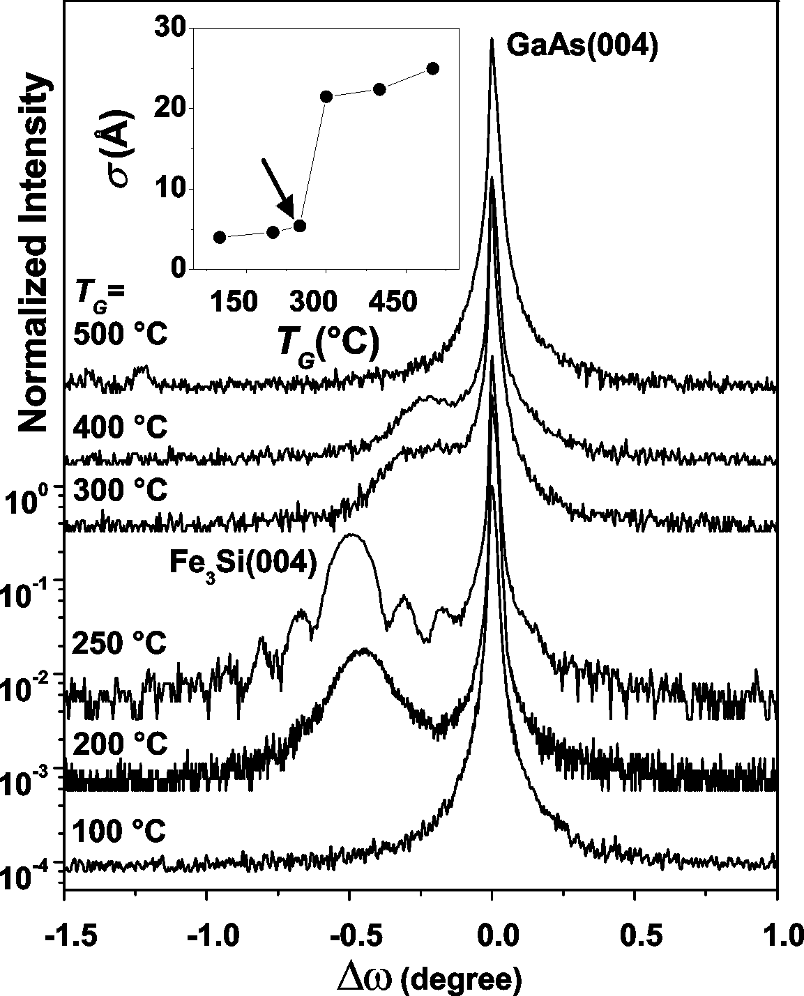
Figure 1 shows normalized skew-symmetric w-2q scans
near the GaAs(004) reflection for Fe3Si films grown at
different growth temperatures from 100 to 500 °C. The
measurements were performed with an analyzer crystal in the
diffracted beam optics. The sample grown at 100 °Cdid not
show any layer peak in the w-2q scans nor any RHEED
pattern during growth, implying that the layer is amorphous.
Though the samples grown at TG= 200, 250, 300, and
400 °C, show a layer peak due to the Fe3Si(004)
reflection, only the sample grown at 250 °Cshows distinct
interference fringes, indicating a high structural ordering and an
abrupt interface [2]. However, the temperature
window where these fringes are observed is much narrower compared
to that on GaAs(001), indicating a narrow growth temperature
window for GaAs(113)A substrates. Most importantly, the epitaxial
orientational relationship of the sample grown at
TG= 250 °Cand all other samples of Fig. 3, as
determined from HRXRD, is given by
Fe3Si(113)[33[`2]]
|| GaAs(113)[33[`2]]. The same orientational
relationship of Fe3Si on GaAs(113)A is indeed consistent with
our expectation on the basis of the close lattice constants of
Fe3Si and GaAs and it demonstrates the stability of these
films.
For the sample grown at TG=400 °C, we found additional peaks
in long range skew-symmetric w-2q scans (not shown) at
2q = 34.9° and 2q = 73.9°, which are very close to Fe2As(110) and (220)
reflections, respectively [12].
Though the exact chemical composition for this layer at 400 °Cis not known, the
presence of the these additional peaks indicates the formation of
interfacial compounds. No additional peaks were observed for TG £ 300 °C. Nevertheless, this implies that the growth of
Fe3Si films on GaAs(113)A
can be performed at a much higher temperature compared to Fe on GaAs. Noteworthy, the optimum growth
of Fe3Si on GaAs(113)A takes place at the same TG
(though the range is much narrower) as for Fe3Si on
GaAs(001), whereas to grow Fe films on GaAs(113)A a lower
TG was required [6]. The root mean square (RMS) roughness of the films has been
determined by atomic force microscopy (AFM) and is plotted vs
TG in the inset of Fig. 1. Fe3Si films with
TG £ 250 °Cexhibit minimized RMS roughness values of
about 5-6 Å (measured over a 5×5 mm2 area).
A significant increase of RMS roughness occurs for
TG > 250 °Cin agreement with the degradation of the
films observed in HRXRD. For TG=500 °C, neither a layer
peak nor any additional peak was observed in the
skew-symmetric w-2q scans. In fact, the AFM
image of this sample shows the formation of a large number of
pyramidal-shaped nanocrystals indicating a three-dimensional
growth mode.
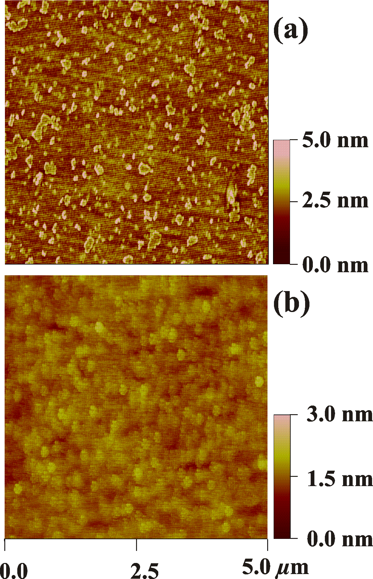
The RMS roughness of the films can be reduced even further by
lowering the growth rate of the Fe3Si layer. This is
demonstrated in Figs. 2(a) and (b) which show AFM images
of two samples grown at 250 °Cwith a growth rate of 0.26
and 0.13 nm/min, respectively. It should be noted that for the
experiments in Fig. 1, the Fe3Si growth rate (as
determined from thickness calibration) was maintained at about
0.26 nm/min. For the lower growth rate (Fig. 2(b)), the
RMS roughness is reduced from 5 to 1.6 Å (measured over a
5×5 mm2 area). Moreover, the growth rate reduction
also improves the magnetic properties. We will return to this
point later. To summarize the difference in growth conditions of
the Fe3Si films on GaAs(113)A substrates, the optimized
growth temperature range is narrower and the growth rate is lower
compared to the growth on GaAs(001).
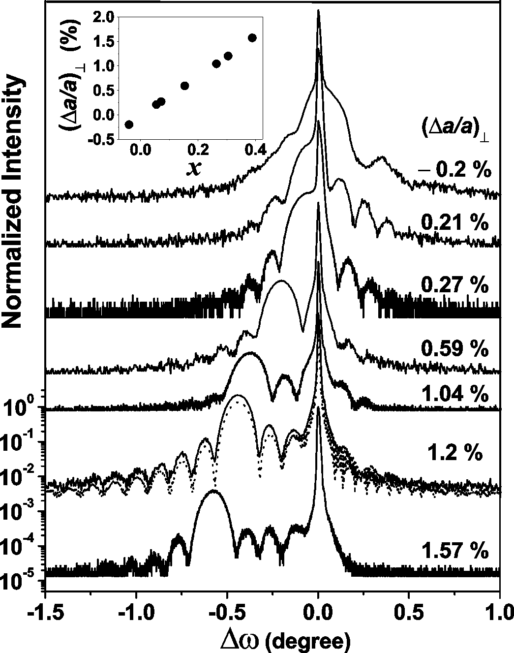
The phase boundary of the bulk Fe3Si
covers a range from 9 to 26.6 at.% Si [13]. To
examine the stability of the Fe3Si phase in this range, the
Fe-Si composition was varied using the above optimized growth
conditions. For simplicity, we kept the Fe cell temperature
constant and varied the Si cell temperature. Figure 3
summarizes the results of HRXRD on these samples. The high crystal
and interface quality of these films is again reflected by the
presence of a large number of interference fringes for all
samples. For a quantitative comparison, we have included a
simulation [14] of the rocking curve using the
Takagi-Taupin formalism for the Fe3Si layer with
perpendicular lattice mismatch (Da/a)^ = 1.2 %. Fit
parameters are (Da/a)^ and the layer thickness d,
taking into account only the instrumental broadening of the
diffractometer. The agreement with the experiment is excellent.
The full-width-at-half-maximum along the (004) Bragg reflection of
the layer is as low as 0.14° for this 40 nm thick film. In
Fig. 3, the Fe3+xSi1-x peak systematically
shifts with respect to the GaAs(004) main peak indicating a
different lattice constant of the layers. Here x denotes
the deviation from the exact stoichiometry. As the Fe/Si flux
ratio is varied around stoichiometry, any excess Fe will
substitute into Si lattice sites and vice versa, leading to
different lattice constants of the layers [15]. It
should be mentioned that with increase of the Si content, a slight
degradation of the films is observed which becomes apparent from
the reduced number of interference fringes in the uppermost curves
of Fig. 3. From the peak separation, (Da/a)^ of the layers was determined, which varies from
1.6 % to -0.2 %. All layers are found to be tetragonally
distorted with a parallel lattice mismatch less than 0.05 %, as
evidenced by HRXRD profiles of asymmetric (004) Bragg reflections
in grazing incidence geometry (not shown here). The composition of
these films was determined from (Da/a)^ using the
method described in our previous work on the GaAs(001)
system [2]. The Si content obtained from this
method was found to be in the range of 15-26 at.%, which lies
within the phase boundary of the Fe3Si phase covering a range
from 9 to 26.6 at.% Si. [13] The inset in
Fig. 3 shows the correlation of x on (Da/a)^. Thus films with exact stoichiometry can be obtained
for almost lattice-matched films.
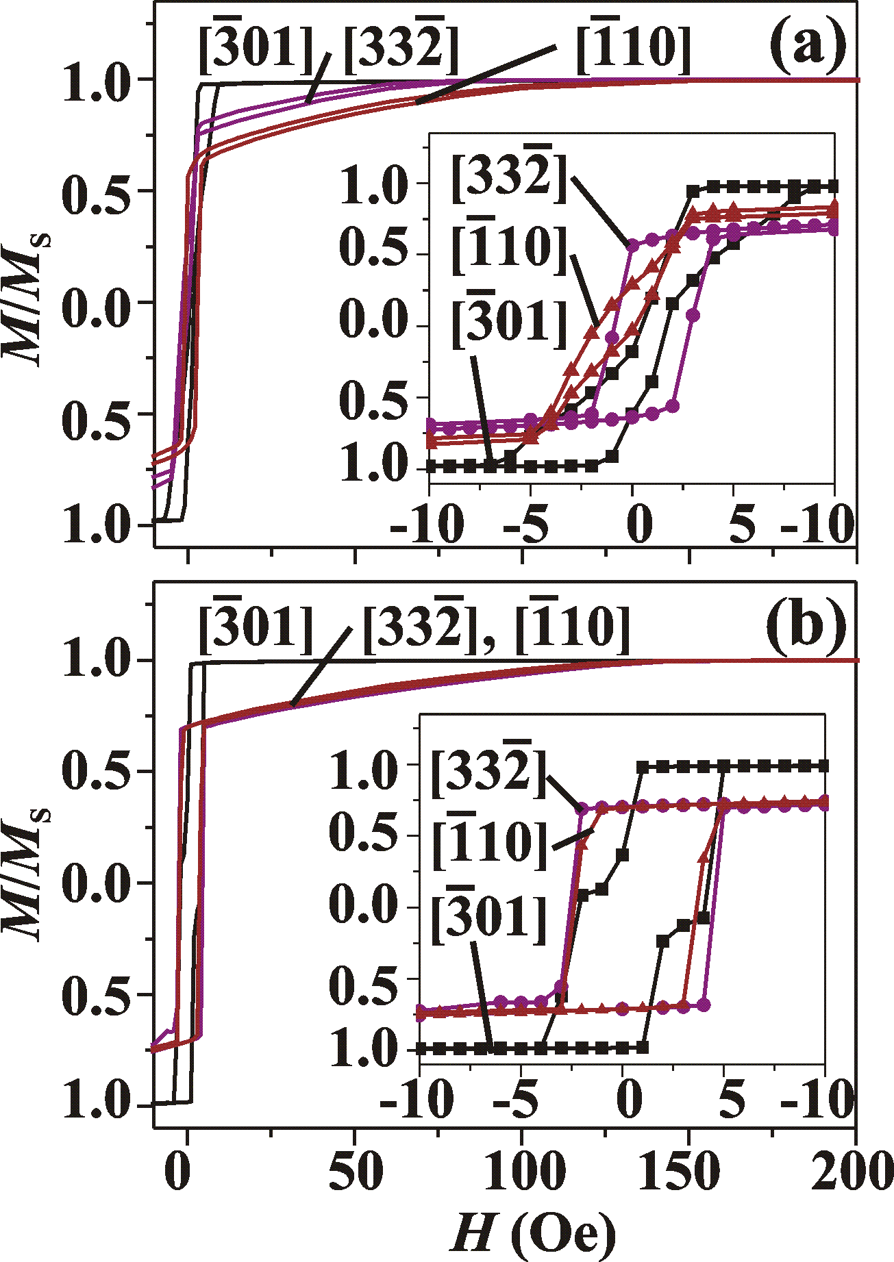
The magnetic
properties of these Fe3Si films were studied ex-situ using superconducting quantum interference device (SQUID)
magnetometry. We will discuss the magnetic properties of a typical
Fe3Si layer exhibiting superior structural properties and
study the effect/requirement of the low growth rate.
Figures. 4(a) and
(b) show room temperature (RT) magnetization curves for the corresponding samples in Fig. 2(a) and
(b), respectively, representing different growth rates. The composition of the two films is comparable (x=0.39 and 0.33 for Figs. 4(a) and
(b)). Both the samples are ferromagnetic at RT and exhibit a dominating in-plane four-fold magnetic anisotropy, with the easy axis
along the á03[`1]ñ directions. The two major
in-plane crystallographic inequivalent directions, namely
[33[`2]] and [[`1]10] are found to be
magnetically equivalent and are intermediate axes. The in-plane
four-fold magnetic anisotropy in these low symmetric [113]
orientated samples arises from the cubic magnetocrystalline
anisotropy, and is a result of the large demagnetization energy in
thin film geometry [16]. Hence, similar to the
case of Fe on GaAs(113)A a reorientation of the bulk easy axis of
Fe3Si, namely á100ñ towards
á03[`1]ñ takes place. The coercive field for
this Fe3Si film (4-5 Oe) in general is lower compared to
that of the Fe films, which also reflects the improved structural
quality of the films. The saturation magnetization (Ms) of
the sample in Fig. 4(b) is (1300±200) emu/cm3,
which is lower compared to bulk Fe (1740 emu/cm3), but
comparable to the value obtained for Fe3Si(001) films with
the same composition [17]. However, the magnetic
reversal of the two samples in Figs. 4(a) and (b) are
different and can be seen clearly in the corresponding insets. For
the sample prepared with higher growth rate, the reversal is
gradual and the switching width is about 5 Oe in all directions as
shown in the inset of Fig. 4(a). On the other hand, the
sample prepared with lower growth rate shows a sharp reversal,
with a switching width of less than 1 Oe. We assume that the
increased switching width in Fig. 4(a) is correlated with
the rough surface morphology in Fig. 2(a). The
interaction between the small particles (as seen in the AFM image)
could be a possible reason for the increased switching width. The
magnetization curve along the [03[`1]] direction in the
inset of Fig. 4(b) shows a two-jump reversal, which is
ascribed to a "nonideal" two-jump reversal similar to Fe
films [18]. The magnetic characterization of all
the other Fe3Si films with varying composition shows
ferromagnetism at RT with a dominating in-plane four-fold magnetic
anisotropy. However, a small uniaxial magnetic anisotropy is also
found superimposed with the four-fold magnetic anisotropy and with
the easy axis lying along the á[`1]10ñ axes
for samples with higher Si content. The low coercive field is
maintained in the studied composition range around the
stoichiometry. A significant decrease of Ms (compared to the
bulk value) is found for the sample with the highest Si content of
26 at.%. More detailed studies of the effect of different
compositions and the growth temperature on the magnetic properties
will be discussed elsewhere.
Our studies shows that high quality Fe3Si films can be grown on GaAs(113)A
maintaining the [113] orientation of the substrate. The growth
conditions are optimized at a growth temperature of 250 °C
and a low growth rate of 0.13 nm/min at which the layer quality is
comparable to the Fe3Si films on GaAs(001) substrates. We
have demonstrated the importance of a low growth rate, which is
more specific to the [113] orientation, to obtain a smooth surface
morphology and superior magnetic properties. The optimized growth
of Fe3Si with varying Fe-Si alloy composition is also
demonstrated around the Fe3Si stoichiometry. All the layers
are shown to be ferromagnetic at RT. The layers exhibit a
dominating four-fold magnetic anisotropy, which arises from the
magnetocrystalline anisotropy and large demagnetization energy of
the Fe3Si films. These studies show the stability of the
high-index surface of a thermally stable ferromagnet, Fe3Si
on a semiconductor substrate. This might be useful for future
device applications.
Acknowledgements
This work is partly supported by the German BMBF under contract
no. 01BM907. The authors would like to thank O. Brandt, L.
Däweritz, and M. Hashimoto for useful discussions and B.
Jenichen for critical reading of the manuscript.
B. Lépine, S. Ababou, A. Guivarc'h, G. Jezéquél, S.
Députier, R. Guérin, A. Filipe, A. Schuhl, F. Abel, C.
Cohen, A. Rocher, and J. Crestou, J. Appl Phys. 83 (1998) 3077.
See FeSi phase diagram in, M. Hansen, Constitution of Binary
Alloys, McGraw-Hill, New York, 1958; R. P. Elliot, Constitution of
Binary Alloys, Suppl. 1, McGraw-Hill, New York, 1965.
For the simulation in the skew geometry, the (004)
reflection of GaAs(113) was approximated by the symmetric (004)
reflection of GaAs(001). For the dynamical x-ray diffraction
formalism used in this simulation see, O. Brandt, P. Waltereit,
and K. H. Ploog, J. Phys. D 35 (2002) 577.
C. Daboo, R. J. Hicken, E. Gu, M. Gester, S. J. Gray, D. E. P.
Eley, E. Ahmad, J. A. C. Bland, R. Ploessl, and J. N. Chapman,
Phys. Rev. B 51 (1995) 15964.
Figure 1: Normalized skew-symmetric
w-2q scans for Fe3Si/GaAs(113)A films with
different growth temperature TG from 100 to 500 °C. The
curves are normalized to the GaAs(004) reflection and are shifted
with respect to each other for clarity. The inset shows a plot of
the RMS roughness s vs TG. The arrow indicates the
optimized growth temperature of 250 °C.
Figure 2: AFM images of Fe3Si films grown at 250 °C,
with a growth rates of (a) 0.26 nm/min and (b) 0.13 nm/min. The
RMS roughness decreases from 5 to 1.6 Å for (a) to (b),
respectively.
Figure 3: Normalized skew-symmetric w-2q scans
for Fe3Si/GaAs(113)A films grown at 250 °Cwith
different Si cell temperature. The curves are normalized to the
GaAs(004) reflection and are shifted with respect to each other
for clarity. The dotted line shows a simulation for a sample with
(Da/a)^=1.2%. The inset shows a plot of x
with (Da/a)^.
Figure 4: Room temperature SQUID magnetization curves along
different crystallographic directions for the samples shown in
Fig. 2 for a growth rate of (a) 0.26 and (b) 0.13 nm/min,
respectively. The insets show the magnified low field regions.
File translated from
TEX
by
TTH,
version 3.68. On 15 Aug 2005, 15:42.