| a. |
An
experiment is performed to investigate the behaviour of a n-p-n transistor
operating in the common emitter configuration. Using suitable diagrams,
state the results you would expect for determining the following characteristics
of the transistor:
i)
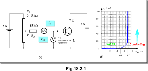
input characteristics, the variation of base current Ib with
the p.d. VBE across the base and the emitter. |
8
marks |
|
Note: Circuit diagrams
not required in all cases. |
|
|
 |
1 |
|
The transistor does not conduct when the p.d.
across base and emitter is less than ~0.5 V. However, when the transistor
conducts, the current is independent of VBE. |
1 |
|
|
|
|
ii)
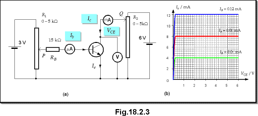
current transfer characteristics, the variation of the collector current
Ic with the base current Ib. |
|
|
|
|
|
 |
1 |
|
When the transistor is conducting and not saturated,
the collector current is proportional to the base current. |
1 |
|
|
|
|
iii)
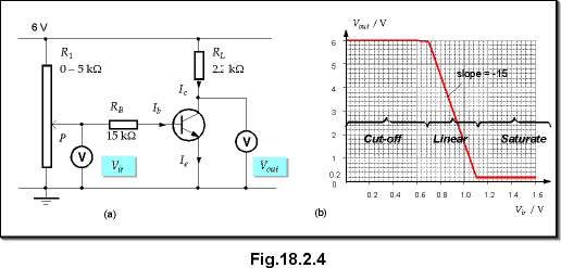
collector characteristics, the variation of the collector current Ic
with the p.d. across the collector and the emitter. |
|
|
|
|
|
 |
1 |
|
When the transistor is conducting, the collector current
is independent of the voltage across C and E, VCE. |
1 |
|
|
|
|
iv)
input-output voltage characteristics, the variation of output voltage Vout
with the input voltage Vin. |
|
|
|
|
|
 |
|
|
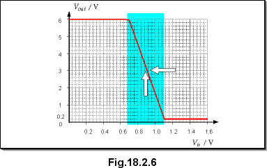
The output voltage vary linearly with the input voltage
for a small range. When Vin is small, the transistor
does not conduct and the output voltage is 6 V. When Vin
is too largel, the collector current reaches the maximum value and the
transistor saturates. The output voltage is ~0 V. |
|
|
|
|
| b. |
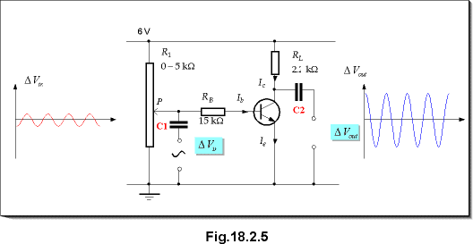
Sketch
the circuit diagram for a linear voltage amplifier which uses a n-p-n transistor
operating in the common emitter configuration. Explain the functions of
the individual components in your circuit diagram. |
6
marks |
|
|
|
|
Linear voltage amplifier |
|
|
 |
2 |
|
1. The potential divider P is
set so that a correct biasing current flows through the transistor. Without
the signal applied, the output voltage is half the voltage of the supply. |
any two
2 |
|
2. The blocking capacitor C1
is to ensure that the baising current is unaffected by the applied signal
which may consist of some d.c. component. |
2 |
|
3. The output capacitor C2 is
to block the d.c. component of the voltage across CE so that the
output from it is a pure a.c. |
2 |
|
|
|
| c. |
From
the graph of the input-output voltage characteristics, explain
i)
how you would prepare the transistor for amplifying a.c. with the smallest
distortion |
2
marks |
|
|
|
|
 |
|
|
In order to ensure that the maximum output
swing DVout without distortion,
the d.c. output voltage should be set at half of the supply voltage. |
|
|
Before the a.c. is applied, carefully set P
to a position so that the output voltage is half of the supply voltage. |
1 |
|
|
|
|
ii)
how the voltage gain of the amplifier is obtained. |
|
|
|
|
|
The voltage gain is obtained from the slope of the Vout-
Vin graph. |
|
|
|
|