PS100 powersupply fix
April 2003 by Daigoro Ookami aka Flemming Steffensen
< Click on any picture for more details. >
|
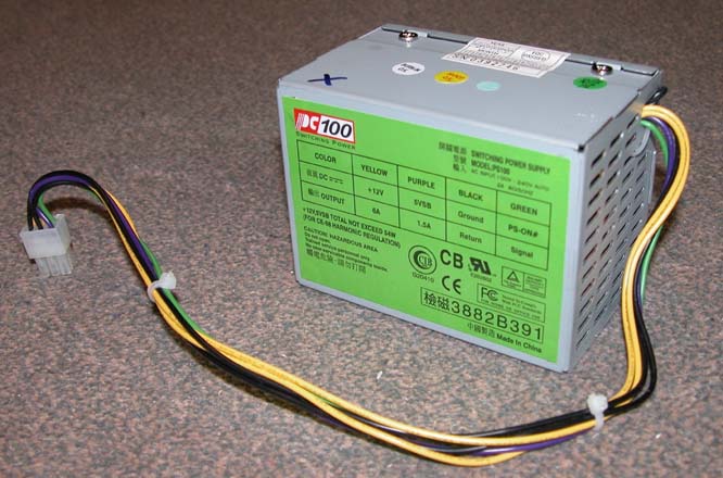
The PS100 power supply contained in the FamilyNet PCs as well as other small consumer PCs and STBs is know to have a manufacturing flaw that will show itself after some time. The flaw affects the voltage output and will make your PC or STB reboot once in a while.
Since the original manufacture of the FamilyNet PCs has ceased to exist, replacements for the PS100 is hard to come by - except if you buy it directly in Taiwan. ComputerCity in Denmark sold a huge quantity of FamilyNet II PCs, and has since tried to get hold of replacement PS100, but these are naturally only for their own customers. For this reason, I decided to do a detailed description of the differences between the flawed and the working power supply, the moment I got my replacements (all five of them) from ComputerCity. All the flawed PS100s I have had was all produced in march 2001. The replacements I have seen was all produced in march 2003. During the two years, the Printer Circuit Board (PCB) has had a slight change to the artwork, and had it's version changed from v3.2 (Artwork #1037) to v3.3 (Artwork #1090). This change only to make room for two power-resistors where the original only had room for one (but had two fitted anyway!). This change has no impact on the functionality of the power supply. Pictures of the change can be found at the buttom of this page. The actual flaw of the PS100 is two capacitors (in this text known as C1 and C2) which should have been specific high speed switching capacitors and not just normal capacitors. The pictures below will show you where these capacitors are located as well as what defects you should look for. NOTE: I was told by ComputerCity that a wrong voltage capacitor had been used, but I found no evidence of this when examining the PS100 power supplies I have available. Naturally this could mean other flaws than the ones described here exists, although I believe that ComputerCity has simply been mis-informed.
|
|||
Overview of the flawed PS100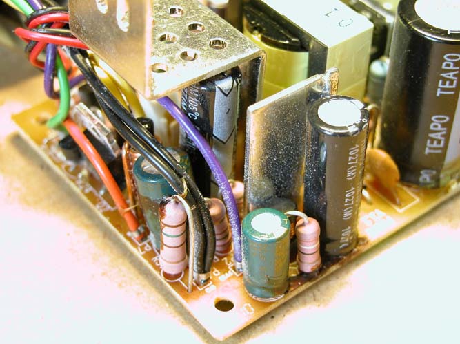
|
Overview of the working PS100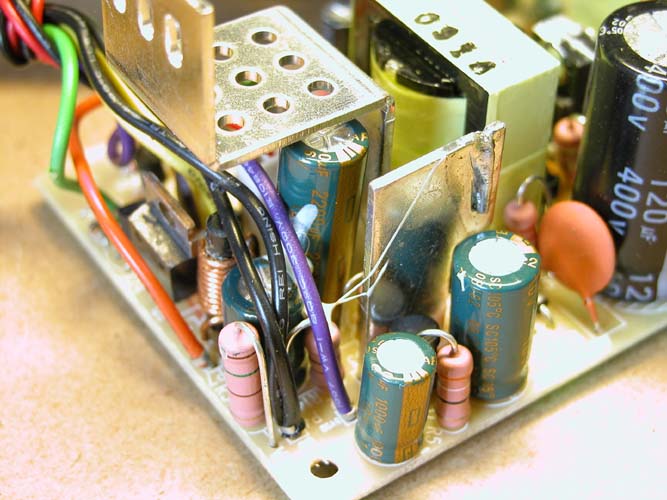
|
||
|
The two pictures above show the area of interest inside the PS100. To the left you can see the flawed power supply, and to the right you can see the working power supply. Notice the two black capacitors on the left picture, which has been exchanged for green high speed switching capacitors on the right picture.
|
|||
Defective C1 - type HM105°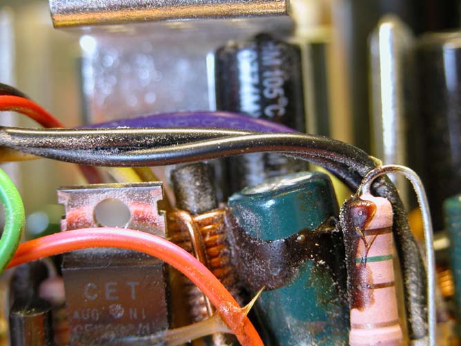
|
Working C1 - type SC105°
|
||
|
To the left, under the heatsink, can be seen the defective capacitor, 2200µF/16V @ HM105°. Notice the destintive bump on top of the black capicator, where it is punctured due to overheating. Due to the heatsink, it's slightly difficult to replace the capacitor, but it can be done without too much work. To the right the new 2200µF/16V @ SC105° high speed switching capacitor can be seen.
| |||
Defective C2 - type HM105°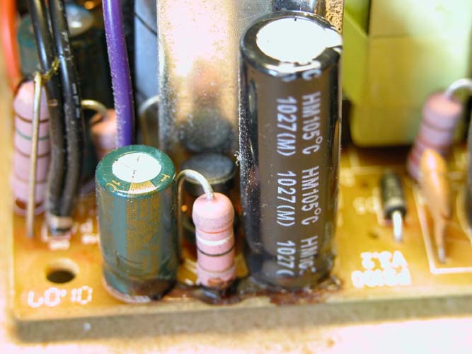
|
Working C2 - type SC105°
|
||
|
To the left can be seen the defective capacitor 2200µF/10V @ HM105°. Notice the unusual crack in the left side of the capacitor, which is possibly due to a weakening of the side during the mounting of the capacitor onto the PCB. Had the capacitor not been exceeding it's temperature specifications due to the high switching frequency, then it would probably have failed at some time soon anyway. To the right the new 2200µF/10V @ SC105° high speed capacitor has been inserted. In the five defective PS100 I had available, only this one had actually leaked.
| |||
The reason why the PCB Artwork was updated.
| |||
Two resistors soldered and glued together.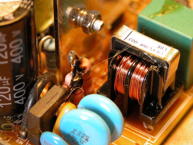
|
Two resistors soldered into the PCB.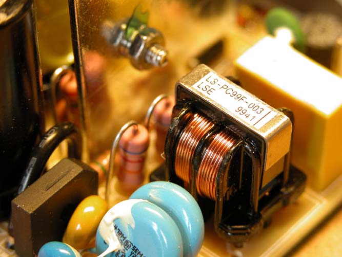
|
||
|
|
||