 |
|
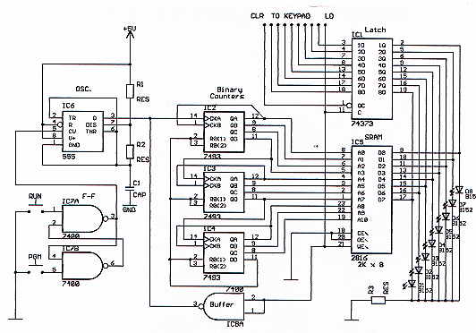
| Circuit Discription: |
| The 555 Osc/timer (IC6) supplies squarewave pulses to the 7493 binary counters (IC's 2,3 and 4) when placed in the RUN mode. The 74373 Octal latch acts as a temporary memory to hold any keypad entries. IC7A and IC7B (Half of a 7400 Nand Gate) form a RS flip-flop which is used to switch the circuit to either Program Mode or Run mode. The LEDs (D1 to D8) act as data monitors. IC5 (2816SRAM) is a 2K by 8 Byte static read and write memory . Data is entered or retrieved one byte at a time via the data pins (D0 to D7). The binary counters IC's 2,3 and 4 are used to open each memory location one byte at a time in response to each pulse it receives from either the 555 oscillator (RUN Mode) or from a Load pulse (LD) entered via the keypad (PGM Mode). |
| Important circuit notes: ------------------------------------------------------------------------------------------------ Contact conditioning as well as load (LD) and clear (CLR) pulses must be supplied by the keypad circuitry. The RUN and Program (PGM) buttons do not require contact bounce conditioning because they control a flip-flop for which contact bounce has no adverse effect other than to re-inforce that a key has bin pressed. |
| Static RAM Programmer: |