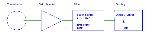
The project is a tremor detector. The detector is able to sense movement through the use of a piezoelectric transducer. The transducer, when is shaken, converts that input energy into electrical signal. The output voltage generated is very low in the range from –0.7V to +0.7V, so it needs to be amplified at least up to 1V or more depending on the input applied to the transducer. This is why we used a gain select. After the signal is amplified, it is filtered, so we get the range in which we are going to operate. The range of operation is from 1 to 10 Hz. The band pass filter will consist of a first order high-pass filter and a elliptic second order low-pass notch filter that will only allow frequencies form 1 to 10 Hz.. This output voltage is inputted to the LM3914 (driver), so the final output could be seen thorough a bar-graph display. A schematic of the entire block diagram is presented below.
The Block diagram consists of the transducer, the gain selector,
band pass filter ,the LM3914, which is the driver for the 10 LEDs bar displayer,
and the Display.
The sensor that we used in this project was a Piezoelectric Transducer. The term transducer is used for a device that converts mechanical energy into output energy. Originally, the term referred to a device that converted mechanical stimuli into electrical output, but it has been broadened to include devices that sense all forms of stimuli, such as heat, radiation, sound, strain, vibration, pressure, acceleration, and so on. It can produce output signals other than electrical, such as pneumatic or hydraulic. Many measuring and sensing devices, as well as loudspeakers, thermocouples, microphones, and phonograph pickups, may be termed transducers.
There are hundreds of kinds of transducers, many of which are designated by the energy change they accomplish. For example, piezoelectric transducers produce electrical signals when subjected to strain or contain a piezoelectric element that produces motion when subjected to an electrical voltage. When the piezoelectric transducer is shaken, then the output voltage generated (a very low voltage) needs to be amplified because it is in the range approximately from –0.7volts to 0.7volts. This is why we used a gain select in our project prototype.
Piezoelectric materials generate charge when squeezed. The amplitude and
frequency of the signal is directly proportional to the mechanical deformation
of the piezoelectric material. The resulting deformation causes a change in the
surface charge density of the material so that a voltage appears between the
electrode surfaces. When the force is reversed, the output voltage is of
opposite polarity. A reciprocating force thus results in an alternating output
voltage. A diagram of the Transducer is shown below:
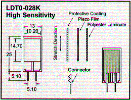
The Properties of a Piezoelectric Film Include:
1.
Wide frequency range: 0.001 Hz to 10
![]() Hz.
Hz.
2.
Vast dynamic range (10
![]() to 10
to 10
![]() psi or m
torr ot Mbar).
psi or m
torr ot Mbar).
3. Low acoustic impedance – close match to water, human tissue and adhesive systems.
4. High elastic compliance.
5. High voltage output: 10 times higher than piezo ceramics.
6. High dielectric strength: withstanding strong fields (75V/mm) where most piezo ceramics depolarize.
7.
High mechanical strength and impact resistance (10
![]() - 10
- 10
![]() Pascal modulus).
Pascal modulus).
8. High stability: resisting moisture (<0.02% moisture absorption), most chemicals oxidants, and intense ultraviolet and nuclear radiation.
The sensitivity of a piezoelectric transducer as a receiver of a mechanical work input is awesome. In its simplest mode the film behaves like a dynamic strain gauge except that it requires no external power source and generates signals greater than those from strain gauges after amplification.
For our project, the extreme sensitivity is largely due to the format of the piezoelectric film material. The low thickness of the film makes in turn a very small cross-sectional area and thus relatively small longitudinal forces create very large stresses within the material. The equivalent model of the transducer is as follows:
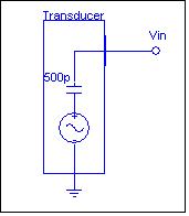
As one can see there is a parasitic capacitance present in
the transducer, and since we are dealing with very low frequencies we will have
to take this into account when designing the input circuit.
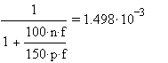
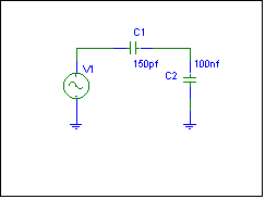
The system needs an equivalent resistance circuit that compensates for the parasitic capacitor present in the transducer. There are varies ways to create an equal theven equivalent circuit. The to create the equivalent circuit and minimize parts, we implemented a capacitive voltage divider. Since the internal capacitance is 150pf, we divide the voltage with a 100nf. The calculation for the equivalent voltage divider is as follows:
![]()


formula
is the voltage divider
Obviously using this method saves a lot of room for other components and shrink down the parts inventory. The second method for creating an equivalent resistor circuit would have to use a 300-Meg ohm resistor and implement a Switched Resistor approach. In this approach, a large resistor (10 Meg-ohm) is placed in series with an analog switch to ground. The control terminal of the switch is driven by a signal of another analog switch that is in series with a 10k ohm resistor, they are connected to positive and negative 9 volts, having a duty cycle of 97 % and inverting their input signal, from a 555 timer. The inversion of the input signal of the first switch allows the second switch to obtain a duty cycle of 3 percent. The duty cycle of that clock signal determines the equivalent linear resistor created by the circuit. The constraints on the clock frequency are as follow:
Req = R/ Duty Cycle
R = Req* Duty Cycle
R= 300M * .03
R =10M
For
linear discharging of the transducer capacitance the product of R*Ct must be 10
times the on time
Ton >= 10*(R*Ct)
Ton>= 10*(10M *0.5E-12)
Ton >= 5E-5 sec
Randomly
6.93E-5 seconds was used for
Ton and it was known that the duty cycle needed to be between 0.3 to 3 percent
Ton =6.93E-5
Duty Cycle = Ton/ (Ton + Toff)
.03 = 6.93E-5 /(6.93E-5 + Toff)
Toff = 2.3E-3
Now to find the resistor and capacitor values of the 555 timer, the calculations are as follow:
Ton = .693 * R2 *C
Let C = .1 u fd
6.93E-5 = 0.693 *R2 *.1u
R2 = 1k ohm
Toff = .693 * (R1 +R2) *C
2.3E-3 = 0.693 * (R1 + 1k) *0.1 u
R1 = 33 k ohm
The equivalent circuit of two different circuit diagrams. The first is a switched resistor and the second is the voltage divider:
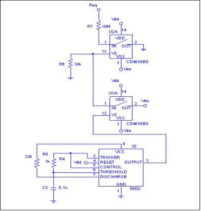
From comparison the capacitive voltage divider is smaller than the switching analog resistor
![]()
The purpose of the gain selector is to amplify the output signal of the
transducer, which is the input voltage of the system, with a high sensitivity of
0.15 volts and a low sensitivity of 1.5 volts. It was needed because the
displayer of the system works with a minimum of 3 volts. The gain selector was
design taking in consideration other future voltage amplifications within the
system, such us the 2 V/V gain of the filter stage. The gain selector was design as a non-inverting amplifier,
using a TLC272 chip with input bias voltages of
+/- 5 V. The circuit diagram of the gain select is shown below:
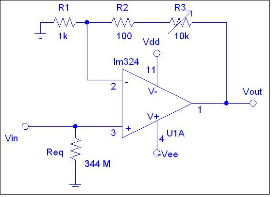
The gain formula for the non-inverting configuration is shown below.
Vout = 3 volts
Vin = .14
Vout = Vin * Gain
3 = (.14 volts) * Gain
Gain = 11 V/V
So since the filter will have 1V/V gain then the amplifier must have
11V/V for the high mode sensitivity, as illustrated in the following
calculation.
Gain Selector Gain * Filter Gain = Total Voltage Gain for High Sensitive Mode
11 * 1 = 11V/V
For the low sensitive mode we used the same technique however we used the low sensitivity voltage of the transducer, 1.5 volts. So we did the following:
Vout = 3.33 volts
Vin = 1.5
Vout = Vin * Gain
3.33 = (1.5 volts) * Gain
3.33/1.5 = Gain
Gain = 1.11 V/V
So since
the filter will have 2V/V gain then the amplifier must have 1.1V/V for the low
mode sensitivity.
Gain Selector Gain * Filter Gain = Total Voltage Gain for High Sensitive Mode
1.11 * 1 = 1.11 V/V
So having this gains we found the resistor for the gain modes for sensitivities
We
arbitrarily found R2, and R1 because they were easy to find
R2 = 100 ohm
R1 = 1 k ohm
For high
sensitivity mode we found Rpot to be:
A = 1 + (R2+Rpot )/ R1
11 = 1 + (100+Rpot)/1k
Rpot = 10k ohm
For low
sensitivity mode we found Rpot to be:
A = 1 + (R2+Rpot )/ R1
1.11 = 1 + (100+Rpot)/1k
Rpot = 10 ohm
Finally simulating it using P-Spice tested the gain selector amplifier, it was tested with the low sensitive mode.
It
can be seen that the input is 0.5 volts and the output is 0 .9 volts having a
voltage gain of 1.1 V/V as expected.
.
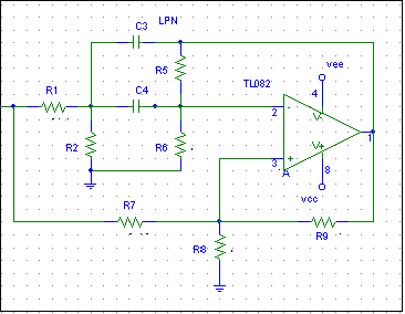
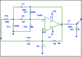
Since the signal produced by the transducer is contained within a band range from 0.001Hz to approximately 10^9Hz, the project contains a second order high pass filter and a first order low pass. Even though the high pass frequency was limited by the response of the transducer itself, it was designed to be around 1.06Hz. The low pass frequency was set to be around 10Hz.
Using the Michael filters program, which I programmed myself, I input the parameters and select the ellipse LPF. The parameters are from 1Hz to 10Hz with attenuation of 3dB and any frequency after 60Hz at –20dB
Below are the zeros and poles of the filter
|
z = 1.0e+002 * 0 + 1.4365i 0 - 1.4365i |
p = -4.0111 + 8.1497i -4.0111 - 8.1497i |
k = 0.0032 |
all the calculations were done by Matlab and by excel.
![]()
![]()
all the calculations were done by Matlab and by excel.
|
|
MATLAB |
|
|
|
|
||
|
K
< 1 |
Qp |
Wp |
Wz
> Wp |
C3(n) |
C4(n) |
P |
R9 |
|
0.0065 |
1.3227 |
57.177 |
902.58 |
100 |
10 |
0.0001 |
10000 |
|
|
|
|
|
|
|
|
|
|
|
|
|
|
|
|
|
|
|
R1 |
R2 |
R5 |
R6 |
R7 |
R8 |
|
|
|
141715.7 |
792958.7 |
2482579 |
10252.04 |
153.8462 |
1.006543 |
|
|
 |
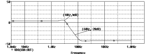
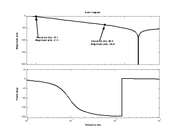
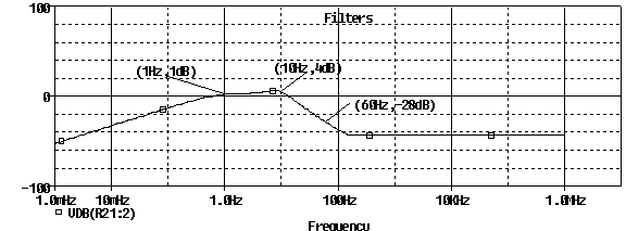
The figure below gives an exact appreciation of the frequency range that our filter provides. It is evident that the cut off frequency for our low pass response is 10Hz and for the high pass response is approximately. 99Hz.
The display stage consists of a display driver and a ten LEDs bar graph displayer, the display driver is a LM3914 chip, which was recommended by the professor. The implementation of this stage was obtain from the data sheets of the LM 3914 which had a typical application implementation, the data sheet of the LM3914 will be included at the end of this report. The implementation of the driver and the 10 LEDs bar graph display is as follows:
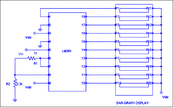
The LM3914 contains an internal
reference voltage of 1.25v between pins 7 and 8. The voltage at pin 7 can be set
by a voltage divider as shown in the figure where Vref= 1.25(1+R2/R1)+
R2IADJ
The Last term R2IADJ can be neglected. The reference high and reference low of the LM3914 being used in the hand tremor analysis system was selected from 0 to 5v. Using the input range equation:
VREF= 1.25(1+ R2/R1)
5= 1.25(1+ R2/R1)
Þ
R2= 3R1
The 10-element LED bar display are the packaged light-emitting diodes attached to the LM3914 in order to provide the visual indication of the input signal level into the display driver. The pin connections for the bar display are shown in the figure above.
The circuit
breaks the input signal range into a string of ten consecutive comparators and
uses LEDs to indicate when the signal falls into the voltage range that is being
compared to which is set by pin 6 of the LM3914. The internal 1K resistance
string partitions the range into the ten comparators, where each of those
comparators causes the corresponding LED to turn on whenever the input
signal’s voltage rises above the reference voltage set by the equivalent
internal resistance at that particular comparator. The upper and lower limits of
the LM3914 bar graph display driver are set by the reference low, Rlo(pin4), and
the reference high RHI (pin 6). The load at pin 7 determines the
brightness of the 10-element LED bar display when connected to the display
driver. Pin 9 determines the mode control, which can be set to be visualized as
either a moving dot or as a bar graph form.
We select R1= 1K and R2= 3.3K using 5% tolerance resistor values
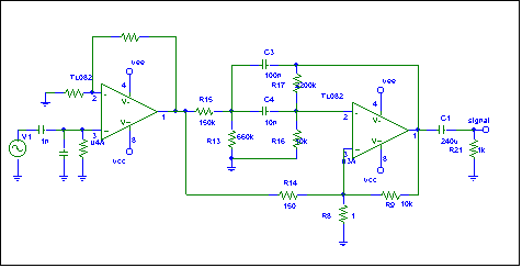
Finally the Schematic of the entire project is shown in the
following page:
![]()