An Introduction to the MAGIC VLSI Design Layout System
by
Jeffrey Wilinski
Table of Contents
Design Rule Checking.............................................. 11
Extraction for Simulation.......................................... 11
Introduction to MAGIC Part II: A Step-by-Step Layout Example of a CMOS Inverter........ 14
Where to go from here:............................................................. 27
REFERENCES.................................................. 27
Table 1
|
Revision
and Change History for c:\my
documents\word\school\general\magic_x3.doc
|
||
|
|
|
|
|
|
|
|
|
|
|
|
|
|
|
|
|
|
|
|
|
|
|
|
This
manual assumes that you:
What
this manual does NOT do:
Conventions
used in this manual:
Although the MAGIC "Command" window is sometimes referred to as the "Text" window, areas are identical. Throughout the history of the MAGIC software, both words have been leisurely used in various application notes interchangeably, so recognize this relationship from the start and become comfortable with it.
Things
you need to know during your first MAGIC session and beyond:
The
<technology file> and our friend the
lambda.
Starting
the MAGIC Software: Command, and Graphics Windows
my_prompt>tap magic
The window that this command was invoked in should give you some type of feedback as to whether your request was successful or not by displaying status information. If no feedback was displayed and a second window did not appear (which is rare but feasible), speak to your neighbor, the TA, or the AITs Help Desk if one is available before going on. Assuming your command was successful, the fresh window should appear labelled as non-other than, "MAGIC". Now type and "enter" the following:
my_prompt>magic [-T<technology filename>] [<file> without any extension tacked on]
in the same window you entered the tap magic command, where <technology filename> is the name of the fabrication technology that the design is intended for, and <file> is the name of the layout file that you wish to edit (this file usually has a .mag extension)[1]. Any valid UNIX filename is acceptable, and if a file with this name does not exist in the current directory, MAGIC will create it. If the technology option is omitted, the layout is done in a generic default technology known as SCNA[2]. Make note that using a generic technology file on a regular basis can add risk to the design, as the desired target technology file may "nullify" portions of your work at a later time because of a process specific layer rule which was violated, or a mask layer call-out that does not exist in that technology.
After MAGIC is initialized two windows should appear on your screen: a graphics (paint) window, and a ">" prompt which appears in a text shell window that accepts commands. The MAGIC program places you in immediate edit mode for the currently invoked file. As your work becomes more advanced and you have multiple files open, you will have to select which window you wish the MAGIC command to act on.
The graphics window is where you draw your VLSI layout and is an ordinary X window that can be moved and resized with the mouse as needed. To work in this area, position your cursor anywhere within the window and click the left mouse button. This makes the graphics window active. Since MAGIC is NOT a menu-driven program, all commands to act on or draw in the layout must be entered in the text or "command" window. (which is the window that MAGIC was started in with the ">" prompt). The mouse should always point within the currently active graphics window when using layout commands as this is the reference point that MAGIC uses to determine where to take action on the command you gave it. Agreeably this is a little odd to always require that the cursor be pointing in the graphics layout window when a command is entered, but as the introduction says, the author makes no excuses for MAGIC behaviour.
The text window is the same window from which you started MAGIC. It is convenient to position this window near the graphics window so that both windows are visible at the same time. All commands you type will appear in the text window as long as your cursor is in a MAGIC graphics window. This interface is slightly awkward, initially counter-intuitive, and takes some getting used to, but becomes routine after a little practice. All error messages pertaining to the design are also displayed in this text window. Commands can be invoked in MAGIC in three ways:
1.By pressing buttons on the mouse in either the graphics or text window.
2.By typing long commands on the keyboard, where long commands are preceded by a colon ":".
3.By typing single-character macros on the keyboard.
If your mouse pointer is in the command window when a command is invoked, MAGIC will ask you to "point to an active window first" as indicated above.
The
Grid, Cursor and the Pointer Tools
While the mouse cursor is used to select, point to, and manipulate objects in the graphics window, the shape of the cursor indicates which of the four available graphic tools is currently in use. Pressing the <spacebar> toggles between the four tools available:
1.The BOX tool is the default tool and is indicated by a crosshair cursor. It is used to position a graphical outline box that layers can be painted and erased in. This is the tool used for all basic drawing tasks and is your layout workhorse. Use of the BOX tool is described below in the Basic drawing section and in more detail in the MAGIC Tutorial #1: Getting Startedand MAGIC Tutorial #2: Basic Painting and Selection.
2.The WIRING tool is indicated by an arrow cursor and is used for advanced drawing tasks such as wiring pads together and a concept known as "plowing". The WIRING section below and the more detailed MAGIC Tutorial #3: Advanced Painting covers certain aspects of this tool in more detail.
3.The NETLIST tool is indicated by a box cursor (not associated with the BOX tool). Reference MAGIC Tutorial #7: Netlist and Routing to cover this tool in more detail.
4.The RSIM tool is indicated by a hand cursor. Reference MAGIC Tutorial #11: Using RSIM with MAGIC for greater coverage of this tool.
We will use the BOX tool most often, which is sufficient for basic editing. The purpose of the BOX tool is to specify a rectangular area of the layout for editing. The left and right mouse buttons are used to position the box. If you click on the left mouse button, the box will move so that its lower left corner is at the cursor position. If you click on the right mouse button, the upper right corner of the box will move to the cursor position, but the lower left corner will not change. The two mouse clicks are sufficient to position the box with arbitrary size anywhere on the screen.
Useful
Global Commands
:quit
quits MAGIC and exits to the shell.
:help command prints out a brief description of all the commands or the specified command.
:load circuit-name loads circuit-name into the window; if circuit-name doesn't exist, MAGIC creates a new empty circuit.
:save circuit-name saves all the changes to the circuit.
:view or v fills the active drawing window with everything painted thus far in the current design.
:grid or g toggles a visible screen grid in the layout area on or off. The grid is useful for lining up various cells, wires, and sections of a schematic. A grid of n lambda by n lambda can be displayed by entering the :gridn command. The g macro is useful shorthand.
:zoomamountzooms in and out of the active window by a factor of amount, i.e. :zoom 2 zooms in twice as much, and :zoom 0.5 zooms out twice as much. The z (small z) macro zooms out to fit the box on the paint window. The Z(uppercaseZ) macro zooms in the same as the ":zoom 2" command.
:paintlayers paints rectangular regions as specified by the box region in the graphical window.
:eraselayers deletes the specified layers from the region within the box.
In each of these commands layers refers to one or more pre-defined layer names separated by commas. In MAGIC there is a unique paint layer and color association for each conducting material, transistor, contact, and combination of materials.
The easiest way to paint and erase is with the mouse buttons.
Method #1, three button mouse: Position the selection box over the area you'd like to paint, then move the cursor over an existing color in your current layout drawing and click the middle mouse button. The color you clicked on should fill the selected area. Alternately to erase everything in a specified area, position a box over that area and move the cursor over a blank spot in the drawing and click the middle mouse button.
Method #2, two button mouse: Follow same procedure as above only emulate the third mouse button by clicking the left and right buttons simultaneously.
Method #3, pallette: A pallette drawing of MAGIC layers has been created by Dr. Newcomb which contains a properly color coded example of the various layers available to you in the MAGIC program. Not all layers are available in every process and are dependent on the technology chosen for the target IC and manufacturer. To use the pallette - which is quite convenient - download it from the UMD Microelectronics Website and call it up from your local MAGIC command window (remember to use the correct path). Although you should not edit this file do not panic if it happens by accident, as it can always be re-downloaded from the website again. Or, you can always make a backup! The most effective way to use this file is to position it in a convenient spot on the screen while editing your layout file in a convenient position, clicking on the appropriate pallette paint layer as required for the task at hand. MAGIC allows you to do this without having the pallette as the active edit window, and will transfer that layer to the active block in the edit window selection area.
Be aware that while you are painting, white cross-hatched sections may occasionally appear and disappear in the layout drawing area. Do not panic: these are design rule violations and will be explained in the Design Rule Checking section.
Examples of various MAGIC layers are listed in Table 1 below, followed by a screenshot in Figure 1 displaying the different colored paint shades associated with them. Note that Figure 1 contains more colors than Table 1 has listed, and your particular layers will vary according to your target process, but your layer color associations should remain consistent throughout.
Table 2: Names and usage ofselected MAGIC layers.
|
LAYER
NAME
|
NUMBER
|
MAIN
ABBREVIATION AND PURPOSE
|
|
bccdiffusion
|
12
|
bd;
buried diffusion for ccd
|
|
capacitor
|
36
|
cap;
poly2 on poly capacitor
|
|
|
26
|
capc;
|
|
colcontact
|
22
|
clc;
npn collector
|
|
col
|
12
|
|
|
cwell
|
45
|
linear
cap option, capacitor well
|
|
ec
|
25
|
poly2contact;
connect metal1 to poly2
|
|
em
|
15
|
|
|
emittercontact
|
16
|
emc;
npn emitter contact
|
|
entransistor
|
42
|
enfet;
entransistor direct NMOS using poly
|
|
eptransistor
|
48
|
epfet;
direct PMOS using poly2
|
|
gc
|
8
|
|
|
glass
|
7
|
cuts
in overglass
|
|
metal1
|
1
|
m1;
first metal layer
|
|
metal2
|
3
|
m2;
second metal layer
|
|
metal
contact
|
2
|
via,
m2contact; connect metal1 to metal2
|
|
metal3
|
5
|
m3;
third metal layer (selected technologies)
|
|
metal
contact
|
4
|
m3c;
metal2 to metal3 contact (or vice-versa)
|
|
nbccdiffusion
|
13
|
I/O
for ccd
|
|
nbccdiffcontact
|
14
|
nbdc;
contact for ccd
|
|
ndcontact
|
23
|
ndc;
metal1 to ndiffusion contact
|
|
ndiffusion
|
33
|
ndiff;
NMOS channel material
|
|
ndop
|
29
|
|
|
ntransistor
|
32
|
nfet;
NMOS device
|
|
nfloating-gate
|
43
|
nffet;
NMOS floating gate
|
|
nncontact
|
22
|
nsc;
metal1 to nsubstratendiff contact
|
|
nohmic
|
32
|
nsd;
substrate contact guard rings
|
|
nwell
|
44
|
for
PMOS substrates
|
|
|
9
|
open
color at this time
|
|
pad
|
6
|
unprotected
pad for external connection
|
|
pbase
layer
|
17
|
pb;
npn transistor base, a.k.a. "P in n-well"
|
|
pbasecontact
|
18
|
pbc;
npn base contact
|
|
polycontact
|
24
|
pc;
poly to metal1 contact
|
|
pdcontact
|
27
|
pdc;
metal1 to pdiffusion contact
|
|
pdiffusion
|
37
|
pdiff;
PMOS channel material
|
|
pdop
|
49
|
|
|
ptransistor
|
47
|
pfet;
direct PMOS
|
|
doubleptransis
|
39
|
PMOS
floating gate
|
|
polysilicon
|
34
|
poly;
gate material
|
|
polysilicon2
|
35
|
poly2;
gates and capacitors
|
|
ppcontact
|
28
|
psc;
metal1 to psubstratepdiff contact
|
|
ppdiff
|
38
|
psd;
substrate contact, a.k.a. guard ring(s)
|
|
pstop
|
19
|
|
|
pwell
|
46
|
NMOS
substrates
|
|
wcap
|
41
|
|
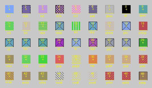
Some layers are created by crossing two layers. For example drawing poly over ndiff (or vice versa) will produce an n-fet. Contacts between layers are made by placing the box over the region of the contact and by painting the appropriate contact. For example, to create a contact between ndiffusion and metal1 layers, place a box over an overlap between the two layers and type the :paint ndc command.
For a complete listing of the layers currently available to you, enter the :layers command in the MAGIC command window.
Basic Drawing
Clickingon the left mouse button positions the lower left corner of the box, while
:move (macro t), and macros q, w, e, and r move the selection by 1-lambda in different directions;
:stretch (macro T), and macros Q, W, E, and R stretch the selection in different directions;
Table 3: Summary of Movement Macros
|
COMMAND
and MACRO (if appropriate)
|
USAGE
|
|
|
move
selection area left
|
|
|
move
selection area down
|
|
|
move
selection area up
|
|
|
move
selection area right
|
|
|
stretch
selection left
|
|
|
stretch
selection down
|
|
|
stretch
selection up
|
|
|
stretch
selection right
|
:upsidedown
:sideways
:clockwise
:copy
(macro c)
:delete (macro d)
:erase
The best way to learn these commands is to try them out. Often you may want to restore things after you've made mistakes using:
:undo (macro u)
or
:redo (macro U)
Make sure that you delete any paint that you don't want. Painting over something with another color just adds more layers, and your original paint will still be there underneath.
You can use the "." (dot) macro to repeat the last command.
The easiest way to move around the graphics window is to use the "," (comma) macro, which centers the window around the cursor position, together with the :zoomn command, (or z and Z macros) to zoom in and out.
Basic drawing is explained in more detail in the MAGIC Tutorial #1: "Getting Started" and the MAGIC Tutorial #2: "Basic Painting and Selection".
Labels
In order to make your layout readable and prepare for extraction and simulation, you need to label your work. Initially decide where you want your label placed in the circuit and what it will say, then left click and immediately right click the pointer center at that spot. You should end up with a small cross (+). It is important to obtain a small cross at the cursor mark but not catastrophic, as you will still be able to label your design but may suffer in the future by having label "boxes" as opposed to label "anchors". After the spot is selected, type:labellabelname
where labelname can be any valid UNIX designation, but a good convention is to use labels that will correspond to circuit signals and make the layout more readable in a printout. In particular, it is necessary to label the supply wires (nodes) as Vdd! and GND! typed exactly as indicated. The ! mark -commonly known to programmers as "bang" - indicates that the node is global and spans the entire drawing. Why one label is all caps and the other not is a matter of constant debate and dates back to some obscure historical origin that not even the finest of long-hair internet hackers can agree on. The manual comments on this particular issue because it is one of the first and most commonly asked questions of new MAGIC users and will spare the author excessive e-mails.
How
to Wire a Circuit
Switch to the WIRING tool by either typing :tool or pressing the spacebar until you get there. Recall that the WIRING tool is indicated by a right pointing arrow in the graphical window. Left click on the paint where you would like the "wire" to start from. MAGIC will automatically select the width of the wire to be the largest box that can fit in the paint you just clicked on. Now "right-click" where you would like the wire to end. The WIRING tool only paints in horizontal and vertical directions. Experiment by painting a couple of diagonal segments and observe what happens.
Many times it is necessary to make a contact between different layers. Inherently paint layers are insulated from each other within the die, so MAGIC requires explicit instructions on when and where to make a contact between the layers. To insert a contact, first make sure that the WIRING tool is selected (right pointing arrow cursor). Second, left-click on the first layer where you want the contact to be made, and immediately middle-click on the layer you want to connect to. The layers don't have to be overlapping to begin with, but they must be immediately next to each other in order for a physical contact to be made which will appear on the screen.
Wiring methods and other advanced drawing techniques are explained in more detail in the MAGIC Tutorial #3: "Advanced Painting (Wiring and Plowing)".
Design
Rule Checking
Design Rule Checking is performed automatically in MAGIC and is one of its most powerful features. MAGIC knows certain rules that your layout should satisfy so that the IC can be fabricated without errors from the <technology file>. In general, design rules specify how far apart various layers must be, or how large various aspects of the layout must be for successful fabrication, given the tolerances and other limitations of the fabrication process. As you lay out the circuit, any time you place wires too close together, paint a block too narrow, or make any other rule violations, MAGIC lets you know immediately by splattering small white dots around the area of concern. Once the error has been corrected the dots will disappear. For example, :paint a pair of metal1 wires ten lambda apart. Next, select one of the wires and move it closer to the other. The white dots will appear once the wires are fewer than 3 lambda apart. In general, you can find out what design rule is violated by clicking the cursor on the white-dots area and by typing :drc why or using the macro "y".
Design rule checking is explained in more detail in the MAGIC Tutorial #6: Design-Rule Checking.
MOSIS Scalable CMOS (SCMOS) Design Rules specify the complete set of design rules defined by the MOSIS VLSI fabrication service and a source to their origin can be found in the reference section at the rear of the tutorial.
Extraction
for Simulation
:extract
produces a separate .ext file for each .mag file in a hierarchical design. If your MAGIC layout is just a single cell named my_cellname.mag, the extraction output will be placed in the file my_cellname.ext. If your layout includes subcells, you can extract all the edited subcells with the command:
:extract all
Alternatively to extract just the selected (current) cell, type:
:extract <cellname>
The output will be placed in the file cellname.ext.
Extraction
is explained in more detail in the MAGIC Tutorial #8: Circuit Extraction.
The
output .ext file is used to generate a netlist file suitable for
simulation.
Introduction
to Cell Hierarchies
Start a new circuit as you learned above. Then, type:
:getcell <name> -- includes a cell that you want in the new circuit.
The included cells are shown as "black boxes" with only the instance names showing with no details of the included cell shown. This is known as the unexpanded form of cells.
You can select and manipulate each cell as you could a box of painted layers. In order to "connect" cells together, you need to know where the "connection points" of a cell are. Thus, you must expand the cell(s) and paint wires between appropriate points of the design. The following macros are used to :expand or :unexpand selected cells:
x - expands a selected cell, making all internal details visible.
X - unexpands a selected cell, making all internal details hidden.
If you included a number of pre-designed identical cells and you want to make a small change to all of them, you can edit just one of the cells by itself and the changes will be reflected in all the other cells. To edit the cell, type:
:loadpath/<cellname>
and MAGIC will load that cell (and all of ITS sub-cells) into a window. Once changes have been made, :save your changes and :load the circuit you were working on previously. All changes will be reflected in your circuit's cells.
Although a more detailed explanation of cell hierarchies can be found in the MAGIC Tutorial #4: Cell Heirarchies, it is recommended that extreme caution be observed in the use of this technique. A minor change to a cell can have disastrous effects on a large design in many areas.
Please follow along now with Part II: A Step-by-Step Layout Example of a CMOS Inverter.
Introduction to MAGIC Part II: A Step-by-Step Layout Example of a CMOS Inverter
The following is a step-by-step example of how to perform a VLSI layout of a basic CMOS logic inverter as shown below in the following schematic diagram:
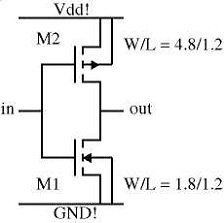
Figure
2: Schematic of Basic CMOS Inverter
The inverter consists of an NMOS transistor M1 and a PMOS transistor M2. The channel width W and the channel length L of the two devices are indicated in um. Note that the source and the body (p-substrate) of the NMOS fet are connected to the ground (GND! node), while the source and the body (n-well) of the PMOS fet are connected to the positive supply (Vdd! node). We assume that the target fabrication technology is the AMI 1.2u CMOS process. The <technology file> name is "scna.60". The unit length lambda for this technology is lambda=0.6um.
We will use basic MAGIC drawing commands to layout the inverter. Remember that you can undo mistakes up to ten deep by typing :undo or u in the command window.
Start MAGIC from the UNIX prompt as described in Section 1 by typing:
my_prompt>magic -T scna.60 inverter
Expand the resulting graphics window over a portion of the screen, but not so large that you cannot see the text window prompt where commands are entered. Remember that the graphics window must be active and the cursor must always point to the graphics window when entering commands. Zoom out and activate the lambda grid so that it is easier to see what you are doing. Type:
:zoom 0.5
and
:grid 1
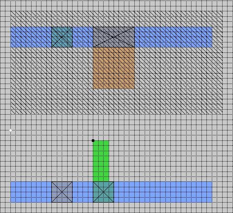
The order in which layers are painted in the graphics window is not important, so the layout steps described here are a recommended guideline as opposed to etched-in-stone rules. Since the device channel width W and length L are specified, you can start by painting the device active areas first: p-diffusion (brown) for the PMOS fet and n-diffusion (green) for the NMOS fet.
The PMOS transistor has a channel width of W=4.8um, which is equal to 8 lambda (i.e. (4.8/.6) in our selected technology. The channel length L=1.2um equals 2 lambda using the same reasoning. The design rules specify that we need at least 4 lambda for the source and drain contacts, plus at least one lambda between the poly gate and the source/drain contacts. Using left and right mouse clicks, shape a box 8 lambda wide and 2+4+4+1+1=12 lambda high. The command:
:paint pdiff
paints the PMOS active area (p-diffusion) in this area. The NMOS transistor has the channel width W=1.8um, which is equal to 3 lambda, and the channel length L=1.2um (2 lambda). Make a 3 lambda (width) by 12 lambda (height) box under the p-diffusion area painted in the previous step. You may want to align the left edge of the box with the left edge of the p-diffusion area. The command:
:paint ndiff
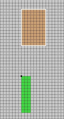
Figure 3: Initial Layout
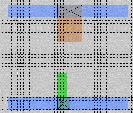
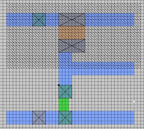
paints the NMOS active area (n-diffusion). A design rule is that n-diffusion must be at least 10 lambda away from p-diffusion. If you placed the n-diffusion area closer to the p-diffusion area, white dots will appear indicating design rule violation. To move the n-diffusion area farther away, point to the area, type the macro "s" to select the area, and use macros q, w, e, or r to move the area until the white dots disappear. At this point, your layout should look something like Figure 3 above. Next, use what you have learned so-far to paint two horizontal, four-lambda wide metal1 wires that will serve as Vdd! and GND! for the circuit. Align the top edge of the Vdd! wire with the top edge of the p-diffusion paint and shape a box 30 lambda wide. The command:
:paint metal1
paints the metal1 (Vdd!) wire in your area (see Figure 4). Next, select the Vdd! wire with the s macro, position the cursor to the lower left corner aligned with the left edge of the Vdd! wire and the bottom edge of the n-diffusion area, and type c. This will copy the metal1 wire to where the GND! wire should be.
:paint pdc
to make a contact between the GND wire and ndiffusion (source of the NMOS), make a box over the overlap between metal1 and n-diffusion layers. Type the command:
:paint ndc
Note that design rules specify that the minimum contact area is 4 lambda by 4 lambda. At this point, your layout should look like Figure 4 below:
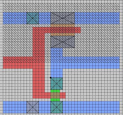
To paint the n-well region place a box extending at least 5 lambda above and below the pdiffusion area and as wide as the metal1 wires. The command:
:paint nwell
paints the n-well for the PMOS fet. At this point, we can also add contacts between the GND! wire and the p-substrate (body of the NMOS fet), as well as between the Vdd! wire and the n-well (body of the PMOS fet). Place a 4-lambda by 4-lambda box over the metal1 wire, but do not overlap the PMOS source contact you already made. The command:
:paint nnc
paints an n-well area to the metal1 contact. If the contact is too close to the pdiffusion-to-metal1 contact, white dots will appear. Select the n-well-to-metal1 contact you just created and use the Q or R macros to move it away until the white dots disappear. Repeat the same to create a metal1 (GND!) to p-substratecontact. Type:
:paint ppc
The layout should now look like the paint in Figure 5 below.
Figure
5: Addition of nwell to CMOS Inverter
The body contacts (such as the ones you just created) should always be located as close as possible to the device source contacts to minimize the possibility of latch-up that plagues CMOS circuits. It is also a good practice to put as many body contacts as possible when space permits.
The next step is to make the fet drain contacts. To connect the drains of the NMOS and the PMOS transistors, paint an output node using metal1. Use the same procedure of steps that you used to create the Vdd!, GND! wires, and source contacts. Note that the simplest way to apply paint in a box is to click the middle-mousebutton over an area already painted with the desired layer in your design. This faster method was previously omitted intentionally, so that necessary experience would be gained in entering and executing MAGIC commands, and the fact that entering paint layers like this may not be the best method in all cases.
You should now have a layout that looks approximately like Figure 6 on the next page.
:paint poly
Notice how the area of poly-to-ndiffusion overlap changes to an area with green/red stripes. This is the channel of the NMOS fet. Create a similar poly box over the p-diffusion area. Correct the size or position of the poly areas if you have white dots indicating design rule violations. Connect the poly areas and make the input node. The current layout should look like Figure 7 on the next page.
The final step is to put labels on the important signal nodes. Execute a left-click / right-click on the poly area, close to the left edge. You should see a small yellow "+" exactly at that spot. To label the "+", type:
:label in
which effectively labels the poly shown as the input node of the inverter. Similarly, label the Vdd! and GND! wires as Vdd! and GND!, respectively, and the output wire/terminal as "out".
 |
 |
The
final layout should appear as in Figure (8) as shown:
|
|
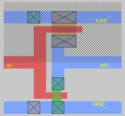
The grid has been turned off using the g macro, and the circuit diagram is shown again for easy comparison with the layout. Now, save the layout that you created with the command:
:save
Extract the layout to create the output file that will be used with a simulator by typing:
:extract
And finally, exit MAGIC by typing:
:quit
You have now been walked-through many of the basic commands of MAGIC, and have layed-out a real circuit. This manual can continue to serve as a guide until the bulk of the commands introduced are committed to memory -- and after some experience, they will be.
From here you will want to reference SPICE manuals containing details on how to simulate your circuits, and consider learning the logic tool that comes with MAGIC known as IRSIM.The University of Berkeley, California has a website dedicated to SPICE[4], and a synopsis is available for IRSIM by typing ":help irsim" at the MAGIC command prompt.
Eventually you will want to explore using Cell Hierarchy in greater detail, and it is recommended that an experienced MAGIC user be consulted prior to start of any major design effort using this method.
MAGIC Tutorials, Summary of Commands, and Complete Manual Pages
MAGIC comes with a set of very old tutorials that go through commands, macros, and mouse functions in more depth than this introduction. Please do not print the tutorials or the manual pages on the VLSI lab printer - these are large files that place burgeoning files in the print que, and can be used on-line as they stand in a new window. For your convenience Jeffrey Wilinski has converted these files to *.pdf format so that they can be viewed with the freeware program Adobe Acrobat either on your SUN Workstation or your PC. Professor Newcomb has made these files available to you on the same webpage that this tutorial is located on.
|
Contents
of the MAGIC Tutorial:
|
Name
of the file to open/download:
|
|
Getting
Started
|
tut1.pdf
|
|
Basic
Painting and Selection
|
tut2.pdf
|
|
Advanced
Painting (Wiring and Plowing)
|
tut3.pdf
|
|
Cell
Hierarchies
|
tut4.pdf
|
|
Multiple
Windows
|
tut5.pdf
|
|
Design-Rule
Checking
|
tut6.pdf
|
|
Netlists
and Routing
|
tut7.pdf
|
|
Circuit
Extraction
|
tut8.pdf
|
|
Format
Conversion to CIF and Calma
|
tut9.pdf
|
|
The
Interactive Router
|
tut10.pdf
|
|
Using
RSIM with MAGIC
|
tut11.pdf
|
REFERENCES
MAGIC
Tutorials 1 through 11, included with the MAGIC release 6.5 software and
listed above in Table 3.