| NANOWALL NANOFLAKE UPDATED DECEMBER 10, 2005 |
| Yihong Wu/NUS Carbon Nanowalls United States Patent Application 20030129305/Wu, Yihong/Priority date=Jan 8, 2002 RB Message 1 RB Message 2 RB Message 3 Three-Dimensional Nanostructured Materials Based on Two-Dimensional Nano-Sheets - WU Yihong Link Fabrication of a Class of Nanostructured Materials Using Carbon Nanowalls as the Templates Y.H. Wu 1 *, B.J. Yang 3, G.C. Han 2, B.Y. Zong 2, H.Q. Ni 2, P. Luo 2, T.C. Chong 1 *, T.S. Low 1 *, Z.X. Shen 3 Link to Advanced Functional Materials article Carbon Nanowalls Grown by Microwave Plasma Enhanced Chemical Vapor Deposition** By Yihong Wu,* Peiwen Qiao, Towchong Chong, and Zexiang Shen Advanced Materials Link Nanowalls/Pictures/Yihong Wu RB Message 4 Yihong Wu RB Message 5 Nanowalls/Other Developments/Doug Baker RB Message 6 |
| NNPP US Patent 6,819,034. Nov. 16, 2004 Inventors: Pavlovsky; Igor (Austin, TX) Assignee: SI Diamond Technology, Inc. (Austin, TX) Appl. No.: 642955 Filed/Priority date: August 21, 2000 CARBON FLAKE COLD CATHODE What is claimed is: 1. An apparatus comprising: a substrate; a film of carbon flakes deposited on the substrate. Press Release Source: Nano-Proprietary Inc. Nano-Proprietary Receives Key Patent Grants Thursday August 26, [2004] 8:45 am ET --Applied Nanotech, Inc. (ANI), today announced that its U.S. Patent claiming two-dimensional carbon nanostructures (dubbed by ANI ``carbon flakes''), with the priority date of August 21, 2000, was allowed by the U.S. Patent Office-- Link to PR Link to USP 6,819,034 RB Message 1 Doug Baker Email RB Message 2 Note - "electrons are coherently scattered from the edge of a flake" N S Xu and R V Latham Dept. of Math. & Phys., Aston Univ., Birmingham, UK Print publication: Issue 3 (14 March 1986) Link |
| Boston College invention (most likely) Nanowalls/ZnO/Optoelectronics/Nanocircuits/Solar Cells, Sensors and Photocatalysis/ nanowire, nanocircuit, nanobelt, tetrapod, nanobridge, nanopin, nanonail RB Message ZnO nanowalls - J.Y. Lao1, J.Y. Huang1, D.Z. Wang1, Z.F. Ren1 , D. Steeves2, B. Kimball2 and W. Porter2 Link US Patent Application 20040105810 Priority Date Sep. 12, 2002 Mentions use as a supercapacitor Link Oregon State University, Hewlett Packard Major advance made in transparent electronics Zinc-tin-oxide thin film transistors Link |
| NNPP (most likely)/CARBON NANOFLAKE/CNF/Texas State of Texas to bring nanoflake technology to market through an (unnamed) Austin-based company. "The University of Texas at Austin Center for Electromagnetic Materials and Devices has been presented with a grant from the State of Texas to bring nanoflake technology to market through an Austin-based company. Aside from the spacecraft and aircraft markets, commercial applications identified include use for health monitoring in commercial buildings, roads, bridges, and any composite materials to increase the integrity of composite skins and structures. They may also be used in advanced antenna designs, signature management, lightning strike protection, and electromagnetic interference protection. The competitive advantage to these sensors is that they do not need to be powered, maintained, connected through wires to data acquisition systems, and are small enough to be embedded virtually anywhere without having any effect on the properties of the embedding material or its behavior. Link (Look for - Title: Nanoflake Sensors - ) |
| Osaka Gas Company Limited Nanoflake carbon tube useful for electron emitting/ United States Patent Application 20030175462 Nishino, Hitoshi ; et al. September 18, 2003, Priority Mar 15, 2002 JP 2002-71937 RB Message |
| CANON/FLAKY CARBONACEOUS PARTICLE AND PRODUCTION METHOD THEREOF Priority date April 4, 2003 Link RB Message |
| University of Manchester/Geim/Graphene Sheet Transistor/Science RB Message Science article abstract Link Science/Electric Field Effect in Atomically Thin Carbon Films/Novoselov et al Link AZoNano article Link Manchester University release Link Carbon goes ballistic/The holy grail Link Geim/U of Manchester/Graphene sheets/Photos/Papers Link BBC/Radical fabric is one atom thick Link Science News/Graphite in Flatland: Carbon sheets may rival nanotubes Link MIT Technology Review article - Ultrathin Carbon Speeds Circuits Link University Of Manchester Intellectual Property Limited Spin out Page Link Two-dimensional atomic crystals Link to article Link to PNAS abstract |
| Center Of Super-Diamond and Advanced Films (COSDAF) Uniform carbon nanoflake films and their field emissions N. G. Shang, F. C. K. Au, X. M. Meng, C. S. Lee, I. Bello and S. T. Lee, Department of Physics and Materials Science, City University of Hong Kong, Tat Chee Avenue, Kowloon, Hong Kong SAR, PR China Received 28 January 2002. Available online 14 May 2002. Link |
| Georgia Tech Ultrathin carbon speeds circuits Researchers at the Georgia Institute of Technology have devised a method for growing ultrathin graphite films by depositing a vapor of carbon atoms on a silicon-carbon crystal surface. The Georgia Tech researchers have made films three atoms thick and several millimeters wide. Link Posted on the arxiv physics archive at arxiv.org/abs/cond-mat/0410240 Link |
| Matsushita/Graphite-Graphene sheets/Electron emitter Priority date April 22, 2003 Link |
| NEC United States Patent Application 20040217382 Kind Code A1 Konuma, Kazuo November 4, 2004 Priority date August 1, 2001 Electron emission film and electric field electron emission device [0222] A description will be made of the eleventh embodiment of the present invention. This embodiment is concerned with the electron emission film of a graphite film (not shown). The graphite film does not have minute projections but has exposed potions where a work function is small in places on its surface. That is, the graphite film is a film on which areas where a work function is small are scattered. Link |
| University of Virginia Synthesis and Field Emission Testing of Carbon Nanoflake Edge Emitters Holloway, Wang "These flake-like structures with ultra sharp edges and large surface area may be promising materials for use in the electron emission and electrochemical fields." Link Brian Holloway, Jianjun Wang � �Synthesis and Field Emission Testing of Carbon Nanoflake Edge Emitters�, provisional application filed October 2003. � �Nitrogen Doped Carbon Nanoflake Field Emitter Synthesized by RFI PECVD on Patterned Nickel Catalyst Layer� 2003 International American Vacuum Society (AVS) Symposium, Baltimore, MD 2003 (talk presented by Jianjun Wang Nov 2003) Link IEEE/Synthesis and field emission testing of carbon nanoflake edge emitters Jianjun Wang Zhu, M. Xin Zhao Outlaw, R.A. Manos, D. Holloway, B.C. Mammana, V.P. Dept. of Appl. Sci., Williams & Mary Coll., VA, USA Abstract: Nanometer edged carbon structures, carbon nanoflakes (CNF), have been synthesized on 50-150 nm diameter nickel arrays. Scanning electron microscopy shows CNF preferentially growing on the Ni dots with the irregular carbon flakes standing perpendicular to the substrate. Raman spectra of this structure show a typical carbon feature with D and G peaks at 1350 and 1580 cm/sup -1/, respectively. Preliminary results of field emission testing, including field emission spectroscopy, I-E curves, Fowler-Nordheim plots and stability curves, indicate that this structure could act as a conductive, robust, edge emitter. Link The Virginia Nanomanufacturing Initiative Nanoporous materials. Materials have been developed with enormous internal surface area through controllable nanopores. A leading example is the aerogel material produced in Norris� laboratory at UVA. Others include the novel carbon nanoflake material being produced by Holloway and Manos and the nanoclay particles under study by Vold at CWM. Such materials have many existing properties in their own right � such as extraordinary dielectric, optical, chemical, acoustic and thermal properties, but can further be functionalized by controlled incorporation of active elements within the pore array. Applications include biological sensors and assaying, novel compound magnetic materials, and integrated optically active semiconductor nanostructures. Link |

|
| Growth of Epitaxial Nanowires at the Junctions of Nanowalls Hou T. Ng,1,2* Jun Li,1,2 Michael K. Smith,1 Pho Nguyen,1,3 Alan Cassell,1,2 Jie Han,1,2 M. Meyyappan1 1Center for Nanotechnology, 2Eloret Corporation, NASA Ames Research Center, Moffett Field, CA 94035, USA. 3Department of Chemical Engineering, San Jose State University, CA 95192, USA. *To whom correspondence should be addressed. E-mail: [email protected] Brevia Link Science Magazine Link - (Easier to read/Better Format!) (Requires 'Sign in') |
| Nanalyze Postings - Graphene Sheets Link |
| The United States of America as represented by the Secretary of the Air Force Nano-graphitic flakes [AKA carbon nanoflakes] United States Patent 6,815,323 Lu, et al. November 9, 2004 [snips] Assignee: The United States of America as represented by the Secretary of the Air Force, (Washington, DC) FIG. 6 in the drawings shows the crystal structure of the desired nano-graphitic flakes. One flake of this material has a diameter of three to four nanometers and has one atomic layer of thickness. Link - USP 6,815,323 Link - RB posting |
| Printable Field Emitters Limited (Chilton, GB) [Most likely!] United States Patent Application 20040131858 Kind Code A1 Burden, Adrian Paul ; et al. July 8, 2004 Priority date March 13, 2001 -------------------------------------------------------------------------------- Field electron emission materials and devices Abstract Graphite comprises atoms arranged in discrete layers (100). The perpendicular distance between these layers is the `d-spacing` (101). A field emission material is obtained by expanding the d-spacing (102). Such expansion may be achieved by an intercalant that has been introduced between layers of the material. Such an intercalant may reside, or may no longer reside, in the material. The material may be placed in position on a substrate by a printing process, prior to expansion. Such field emission material may be used in cold cathodes in field electron emission devices. -------------------------------------------------------------------------------- Inventors: Burden, Adrian Paul; (Singapore, SG) ; Baigrie, Stephen Michael; (Swindon, GB) Priority Mar 13, 2001 Claims 1. A field electron emission material formed of a material comprising layers of atoms, in which the inter-layer spacing has been expanded. 5. A field electron emission material according to claim 1, wherein said layered material comprises graphite. 20. A field electron emission material according to any of the preceding claims, wherein said material has been placed in position on a substrate by a printing process. 24. A field electron emitter formed from a field emission material according to any of the preceding claims, and arranged to serve as a cathode in a field electron emission device. [0009] Preferred embodiments of the present invention aim to provide improved field electron emitting materials and devices that may be used in devices that include (amongst others): field electron emission display panels; high power pulse devices such as electron MASERS and gyrotrons; crossed-field microwave tubes such as CFAs; linear beam tubes such as krystrons; flash x-ray tubes; triggered spark gaps and related devices; broad area x-ray sources for sterilisation; vacuum gauges; ion thrusters for space vehicles; particle accelerators; lamps; ozonisers; and plasma reactors. [0010] According to one aspect of the present invention, there is provided a field electron emission material formed of a material comprising layers of atoms, in which the inter-layer spacing has been expanded. [0014] Preferably, said layered material comprises graphite. [0116] The operation and construction of such devices, which are only examples of many applications of embodiments of this invention, will readily be apparent to those skilled in the art. An important feature of preferred embodiments of the invention is the ability to print the field electron emission material, when formed as an ink, as an electrode pattern, thus enabling complex multi-emitter patterns, such as those required for displays, to be created at modest cost. Furthermore, the ability to print enables low-cost substrate materials, such as glass to be used; whereas micro-engineered structures are typically built on high-cost single crystal substrates. In the context of this specification, printing means a process that places or forms an emitting material in a defined pattern. Examples of suitable processes are (amongst others): screen printing, Xerography, photolithography, electrostatic deposition, spraying, ink jet printing and offset lithography. Link US Patent Application 20040131858 |
| DuPont Re 'intercalation ' and 'expansion' of graphitic layers see: United States Patent Application 20040017141 Kind Code A1 Cheng, Lap-Tak Andrew ; et al. January 29, 2004 Priority date April 24, 2002 -------------------------------------------------------------------------------- Electron field emitter and compositions related thereto Abstract This invention provides compositions of matter that contain an electron emitting substance and an expansion material. The expansion material may, for example, be an intercalation compound. When a film is formed from the composition, expansion of the expansion material typically causes rupturing or fracturing of the film. No further treatment of the surface of the film is typically required after expansion of the expansion material to obtain good emission properties. A surface formed from such a fractured film acts as an efficient electron field emitter and thus is useful in vacuum microelectronic devices. -------------------------------------------------------------------------------- Inventors: Cheng, Lap-Tak Andrew; (Newark, DE) ; Roach, David Herbert; (Hockessin, DE) Correspondence Name and Address: E I DU PONT DE NEMOURS AND COMPANY Link US Patent Application 20040017141 |
| MITSUBISHI CHEMICAL CORPORATION, FRONTIER CARBON CORPORATION WO 2004/089821, 21 October 2004, Priority date April 7, 2003 CARBON PARTICLE AND METHOD FOR PREPARATION THEREOF From abstract: In a preferred embodiment, the graphite thin film is a thin film formed by the lamination of 5 to 50 layers of a graphene sheet structure, the graphite thin film occupies a space of a thickness of 10 to 1000 nm, and the carbon particle has a BET surface area of 50 to 3000 m2/g. The above carbon particle is a novel substance which has a fine structure of a nano-size and is useful as a functional material. WIPO Link to WO 2004/089821 ESP Link to WO 2004/089821 |
| Motorola Of interest re dendritic form United States Patent 6,087,765 Coll , et al. July 11, 2000 Priority date Sept. 30, 1996 Electron emissive film Abstract An electron-emissive film (170, 730) is made from graphite and has a surface defining a plurality of emissive clusters (100), which are uniformly distributed over the surface. Each of the emissive clusters (100) has dendrites (110) extending radially from a central point (120). Each of the dendrites (110) has a ridge (130), which has a radius of curvature of less than 10 nm. The graphene sheets (160) that form the dendrites (110) have a (002) lattice spacing within a range of 0.342-0.350 nanometers. Link to USP 6,087,765 |
| Nano-Proprietary United States Patent 6,573,643 Kumar , et al. June 3, 2003 Priority date Oct. 2, 2000 (with parents back to Mar. 16, 1992) Field emission light source Abstract A field emission cathode for use in flat panel displays is described including a layer of conductive material and a layer of amorphic diamond film, functioning as a low effective work-function material, deposited over the conductive material to form emission sites. The emission sites each contain at least two sub-regions having differing electron affinities. Use of the cathode to form a computer screen is also described along with the use of the cathode to form a fluorescent light source. Inventors: Kumar; Nalin (Cherry Hill, NJ); Xie; Chenggang (Phoenix, AZ) Assignee: SI Diamond Technology, Inc. (Austin, TX) Appl. No.: 677361 Filed: October 2, 2000 Such a carbon film may comprise several different types of structures, including carbon flakes as disclosed in U.S. patent application Ser. No. 07[09?]/642,955. 17. A light source comprising: a field emitter deposited over a conductive filament; and an anode surrounding said filament, said anode operable for emitting light in response to receipt of electrons from said field emitter deposited over said conductive filament. 23. The light source as recited in claim 17, wherein said field emitter comprises carbon flakes. Link to USP 6,573,643 |
| GrafTech US Patent Application 20040033189 February 19, 2004 Priority date Aug 15, 2002 [0051] The aforementioned inventive methods may be used to form nano-sized expanded graphite particles. A nano-sized particle has at least one dimension that is less than about 1 micron. Preferably, the nano-sized particle has at least one dimension of less than about 100 nm, more preferably less than about 50 nm. In preferred embodiments of the nano-sized particle graphite, preferably the thickness of the particle is less than about 10 nm, more preferably less than about 5 nm, even more preferably less than about 1 nm, and most preferably less than about 0.5 nm. For example, the particle may comprise a single graphene layer. Link to US Application 20040033189 Link to RB posting |
| Some Definitions: Graphite - including Flake Graphite - Link Graphite - Link Graphene - Link1 Link2 Image Gallery - Graphite and Graphene - Link Graphene C62H20, Graphene with adatom C63H20, Graphene with adatom pair C64H20 - Link |
| --Some Background-- Isle Bright Limited/CFB PLC "Non recoverable expenses" "A further �200,000 has been taken as a provision against Management Fees to Isle Bright Limited and its cold cathode technology. The board took the decision in January 2000 to terminate its support due to insufficient market demand." Link ISLE BRIGHT LIMITED PATENT FILINGS 1) WO 99/44215 Filed Feb. 27, 1998 Priority date Feb. 27, 1998 Inventors: OBRAZTSOV, Alexandr Nikolaevich PAVLOVSKY, Igor Jurievich VOLKOV, Alexandr Pavlovich Abstract: The present invention pertains to the field of vacuum electronics and more precisely relates to a field emitter intended for use as an electron source (cathode) in vacuum electronic devices for various purposes such as cathodic luminescent light sources, light�emitting indicators and flat displays for the optical representation of information. The field emitter of the present invention consists in a carbon film whose main portion is made of graphite clusters having their basic crystallographic planes preferably oriented so as to be perpendicular to the plane of the substrate on which said film is located. This emitter exhibits improved emission parameters that enable its use for the above�mentioned purposes. The method for producing this emitter comprises previously applying diamond crystallites on an electro�conductive substrate and depositing graphite clusters on said crystallites in order to obtain a monolithic film. The parameters of the deposition process are selected so that the crystallographic basic planes in the graphite clusters are preferably oriented in a direction perpendicular to the surface of the substrate. These parameters are also selected in order to provide for a modification in the electronic configuration of the carbon atoms in the thin boundary layer so as to reduce the work function of the electrons. WIPO Link to WO 99/44215 Espacenet Link to WO 99/44215 2) WO0040508 Filed Dec. 30, 1998 Priority date Dec. 30, 1998 Inventor: OBRAZTSOV ALEXANDR NIKOLAEVICH Abstract: The present invention relates to a method for producing a film-type carbon material, wherein said material is made of plate-like graphite crystallites or carbon nanotubes which are deposited from a carbon-containing gaseous phase using an electric discharge. The material thus obtained can essentially be used in the production of field emitters or electrodes for electrochemical devices. Espacenet Link to WO0040508 |
| Marubun Corporation/Nagoya University/NU EcoEngineering Co. Asia Nanotech Digest Nano Science and Technology in Asia Countries: Japan, China August/September 2004 12. Marubun Markets Apparatus for Carbon Nanowalls The semiconductor trading company Marubun Corp. has joined with Nagoya University to market an apparatus to synthesize carbon nanowalls. This form of carbon was initially developed in Singapore. Researchers at Nagoya University have succeeded in producing them by a commercial method. These nanowalls emit electrons more readily than carbon nanotubes; thus, they may boost the performance of new-generation field-emission displays. The university group has succeeded in synthesizing carbon nanowalls of varying density, and in thicknesses ranging from several nanometers to tens of nanometers. Marubun has obtained exclusive marketing rights to the technology that has been developed to the commercial stage by the university-affiliated start-up NU EcoEngineering Co. This month, Marubun will begin accepting orders this month for the specially designed apparatus to synthesize carbon nanowalls, each of which is expected to cost approximately 50-100 million yen (US $450-900K). Link to PDF file PLASMA AND NANO Many nanoflake photos. Link to PDF file |
| Shimane Masuda Electronics Co., Ltd. (SME) Nano-Proprietary, Inc. and Shimane Masuda Electronics Sign Development Letter of Intent with Rights to a Joint Venture and/or License Agreement ``We believe that this agreement will greatly contribute to a friendly development between the Shimane Prefecture and the State of Texas,'' said Yuzuru Ishikawa, president & CEO of Shimane Masuda Electronics." Link State of Texas to bring nanoflake technology to market through an (unnamed) Austin-based company. "The University of Texas at Austin Center for Electromagnetic Materials and Devices has been presented with a grant from the State of Texas to bring nanoflake technology to market through an Austin-based company. Link (Look for - Title: Nanoflake Sensors - ) My observations SME intends to promote a friendly development with the State of Texas and the State of Texas has provided (indirectly through the University of Texas at Austin) an unnamed company in Austin a grant to bring nanoflake technology to market. NNPP is the only company in Texas that I am aware of that has nanoflake technology. In view of these facts, I postulate that SME and NNPP may be developing nanoflake technology. SME produces LNFETs (transistors). Nanoflakes would be a terrific base for transistors, as would CNTs. Perhaps that is the SME/NNPP/Texas co-development thrust - nanoflake transistors and/or nanoflake electronics of whatever kind with a CNT involvement. However, I also note that the agreement and PR are quite specific in mentioning "CNT sources". Nanoflakes are not CNTs! So perhaps NNPP/ANI is cooperating with another company on nanoflake commercialization and made it quite clear in the PR announcement and SEC 10QSB filing on Oct. 29, 2004, that CNTs were involved with SME so as to distinguish the SME involvement from any others involving carbon nanoflakes. Link to SEC 10QSB filing This statement in the 10QSB is intriguing: 3-4. For the development of products the Parties will investigate the Canon's and Toshiba�s patents related to the ANI patent licensed to Canon thoroughly so that the Parties can develop the products without any infringement. I find it intriguing because the Canon license dealings with ANI involved ANI's SED technology which does not involve carbon nanotubes at all but involves a carbon film which in view of the SED features creates an electron emission. Canon and Toshiba each have many, many SED patents of their own as well but none have any CNT involvement. So I wonder about SME's concerns. ANI does have carbon flake technology and I can readily see where, because of the film nature of the flakes, SME could wish to ensure that their co-development work with ANI does not infringe on any Canon or Toshiba patents or conflict with the license deal with Canon. Perhaps it is just a general concern by SME that they avoid any difficulties with any Japanese company that has had prior dealings with ANI. So, in view of all of the above I can't quite determine whether the ANI SME agreement involves just CNTs or flakes as well. |
| SME & ANI & Xray Flat Panel Imaging Perhaps this is what SME & ANI are cooperating on! Link to similar activity involving xray flat panel imaging Link to RB message |
| PHILIPS/Carbon Flakes(undoubtedly Carbon Nano Flakes)/FED TV WO2004097883 Link to WO2004097883 Link to RB message 1 Link to RB message 2 Link to RB message 3 This is the first instance I have seen of an application from Philips for applying carbon flakes to a substrate for a FED TV display. The basic patent for nanoflakes on a substrate is held by NNPP with PAVLOVSKY the inventor. Is Philips using 'nano' flakes? Not disclosed - they only identify them as "carbon flakes". See section "NNPP" above. And consider this. The Philip's disclosure says "Suitably, said emitting particles are anisometric particles, such as graphite flakes, rods, wires, carbon nanotubes or a combination thereof." And, "The emitter particles 2 are in this example graphite flakes, but may be constituted by any anisometric particles, such as rods, wires or carbon nanotubes. The graphite flakes, with a nominal size of preferably less than about 4-10 microns, have sharp emitting edges and are favorable with respect to their emitting properties in a field emission device." So - the graphite flakes are favorable compared to nanotubes. I can only conclude that they MUST be carbon nano flakes as the only carbon flakes I know that provide better emission properties than nanotubes are carbon nano flakes! |
| Meijo University, Nagoya University M. Hiramatsu Department of Electrical and Electronic Engineering, Meijo University, Tempaku, Nagoya 468-8502, Japan K. Shiji and H. Amano Department of Materials Science and Engineering, Meijo University, Tempaku, Nagoya 468-8502, Japan M. Hori Department of Electrical and Electronic Engineering and Information Engineering, Nagoya University, Chikusa, Nagoya 464-8603, Japan Fabrication of vertically aligned carbon nanowalls using capacitively coupled plasma-enhanced chemical vapor deposition assisted by hydrogen radical injection Link |
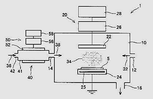
| HIRAMATSU, Mineo; HORI, Masaru ( Meijo University and Nagoya University - most likely) WO 2005/021430 10 March 2005 CARBON NANOWALL PRODUCING METHOD, CARBON NANOWALL, AND PRODUCTION APPARATUS To provide a novel method of producing a carbon nanowall and an apparatus suitable to implement the method. A source gas (32) the constituent elements of which include at least carbon is introduced into a reaction chamber (10). In the reaction chamber (10), parallel-plate capacitive-coupling plasma (CCP) generating mechanism (20) having first and second electrode (22, 24) is provided. With this, an electromagnetic wave such as an RF wave is applied to produce a plasma atmosphere (34) in which the source gas (32) is changed to plasma. In a radical generating chamber (41) installed outside the reaction chamber (10), a radical source gas (36) containing at least hydrogen is decomposed with an RF wave or the like to produce hydrogen radicals (38). The hydrogen radicals (38) are injected into the plasma atmosphere (34), thereby forming a carbon nanowall on the surface of a substrate (5) placed on the second electrode (24). Link to WO 2005/021430 |
 |