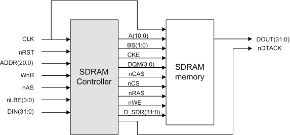
figure 1. system level diagram.
2. Functional description.
Table 1. Interface signals
signal |
name |
active |
I/O |
description |
| CLK | clock | N/A | input | system clock |
| nRST | reset | low | input | system reset |
| ADDR(20:0) | memory address | N/A | input | memory address for r/w access |
| WnR | access type | N/A | input | when low read transfer, when high write tran. |
| nAS | address and data strobe | low | input | starts transfer |
| nLBE(3:0) | input mask for data | low | input | input enable/disable for data |
| DIN(31:0) | data input | N/A | input | data to be written into sdram |
| A(10:0) | address bus | N/A | output | address or control signals into sdram |
| BS(1:0) | bank select | N/A | output | determines bank to which commands are executed |
| CKE | clock enable | high | output | sdram CKE input |
| DQM(3:0) | data mask | high | output | sdram data masks, mask individual bytes during data write. |
| nCAS | column address strobe | low | output | sdram nCAS input |
| nCS | chip select | low | output | sdram chip select |
| nRAS | row address strobe | low | output | sdram nRAS input |
| nWE | write enable | low | output | sdram nWE input |
| nDTACK | transmission acknowledge | low | output | acknowledges data transfer, strobe for data output from sdram |
| DATA_OUT_SDR | data bus | N/A | output | sdram data in bus |
N/A - not applicable.
All signals are synchronous to the system clock, outputs are registered at the controller's outputs.
SDRAM is ready to normal operation after initialization time, which is 100 us for Micron 32x2 MB. SDRAM controller informs host when initialization is completed by driving nDTACK low for one cycle. After that, host can make write/read accesses to memory.
There is no fixed delay for accesses, ie. after driving nAS low, host can't expect that nDTACK will be active(low) after 5 cycles for example. Why? because SDRAM needs refreshing from time to time, and refreshes can intersperse write/read accesses. If it is a problem (ie. read/write timing must be precise with predictable constant wait states) you must manually change source code to give higher priority to accesses than refresh system or use fifo.
User interface to sdram controller is very simple and frees user from issuing complicated commands to sdram memory. The only things user should do are: select access type (write or read), byte mask for data, address and data input and generate address strobe nAS to sdram controller.
Example of write access:
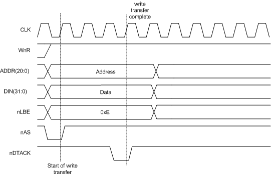
In above example host makes write access to sdram memory using sdram controller. WnR line is set to high (write access), nLBE is set to 0xE (1110 binary which enables writing only to lowest byte of data bus), data and address lines are set valid. Host puts nAS line low, which is address, data and control signals strobe. In next cycle sdram controller "sees" nAS line low and starts transfer. When transfer is finished nDTACK line is low. New transfer can be initiated immediately when line nDTACK is set high after being low, that is:
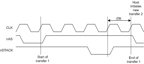
tTR is minimum time between new transfer can be initiated after nDTACK low was sampled and is equal to one clock cycle.
Read transfers are similar from the user side, except that, they are burst so nDTACK low last respectively longer. Below example of four read burst transfer with CAS latency of 2:
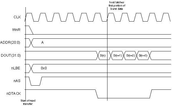
nLBE is set to 0x0 which means that we are writing all four bytes at a time. Host samples nDTACK line after initiating a transfer, and when it is low, host reads data from data bus.
3. Parameters.
There are two designs in files section. One designed for 64 Mbit SDRAMs (32x2 MB), and second, generic design. But generic design wasn't thoroughly tested and may have bugs (only tested with Micron 64Mb). However, both designs have parametrizable timing parameters, CAS latency, clock period and read burst size. In addition to that generic design has much more flexibility by having many more parameters.
Table 2. Parameters.
Parameter |
default value |
units |
description |
available in generic design |
available in non-generic design |
| data_width | 32 | bit | host and sdram data bus width | + |
- |
| rows | 2048 | n/a | number of sdram rows | + |
- |
| columns | 256 | n/a | number of sdram columns | + |
- |
| haddr_width | 21 | bit | host address bus width | + |
- |
| saddr_width | 11 | bit | sdram address bus width | + |
- |
| clock_period | 30 | ns | clock period for controller and sdram | + |
+ |
| burst | 8 | n/a | burst size | + |
+ |
| auto_precharge | low | logic | active high enable autoprecharge | + |
- |
| init_ref_cycles | 2 | n/a | sdram initialization refresh cycles | + |
- |
| tRCD | 65 | ns | ACTIVE to READ or WRITE delay | + |
+ |
| tRP | 20 | ns | PRECHARGE command period | + |
+ |
| tREF | 15000 | ns | Refresh period (1 row!) | + |
+ |
| tRFC | 65 | ns | AUTO REFRESH period | + |
+ |
| tWR | clock_period+7 | ns | WRITE recovery time | + |
+ |
| tSTARTUP_NOP | 100000 | ns | sdram initialization time | + |
+ |
| CAS_latency | 2 | n/a | CAS latency | + |
+ |
Non generic design is slightly faster than generic for VirtexE (143 vs 142 MHz), and much faster for Virtex2 (210 vs 173 MHz).
4. Final words.
This SDRAM controller is fully synthesizable. It was synthesized using Synplify Pro and PAR was done with Xilinx Implement. Code is generic and does not use any architecture specific constructions, so it should work on Altera or other devices.
Maximum speed of core for VirtexE is 142 MHz ( Virtex
XCV2000E -6) with 108 slices used.
Maximum speed of core for Virtex2 is 173 MHz ( Virtex XCV1000 -4) with 77
slices used.
The design was tested on real SDRAM memory included in board with Virtex XCV2000E. It was Micron 64 Mbit (32x2 Mb) (simulation model included in files) and worked. I don't know wheter it will work with others memories or not, and take no responsibility for any damage this controller could do.
CREDITZ: Thanx to Manticore guys, I "stole" process
for generating refresh counts from their sdram controller, as well timing
description way,
so I give them credits here.
Greetz to my girl Eveline.
files:
sdramctrl.zip - non-generic design - designed for 32x2 Mb models (ver. 1.0)
sdramctrl2.zip - generic design (ver
1.0)
