| SCANNING
TUNNELING MICROSCOPY |
|
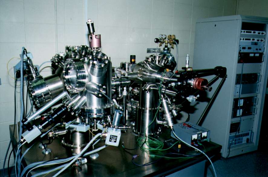
| The Scanning Tunneling Microscope,
or STM, was invented in 1982
by Gerd Binnig and Heinrich Rohrer, and earned them the Nobel Prize
in 1986. The STM in our lab is shown to the right. The animation below illustrates how the STM tip moves over the surface to take an image. The tip is a sharpened metal probe ideally with one atom on its end to produce clearer pictures. The probe is placed extremely close to the surface, approximately a billionth of a meter away from the surface.
|
 |
|
|
How does the STM work? If a voltage is placed between the STM tip and the sample, small particles called electrons (much smaller than atoms) jump or 'tunnel' from the tip to the surface (or vice-versa) and make up an electrical current that can be measured. The closer the tip is to the surface atoms the easier the electrons can tunnel across the gap,thus more current is produced. The great thing about the STM is that you can measure and hold the tunneling current constant. By doing this the tip can be kept the same distance from the surface atoms. If this measured current is smaller than the set current, a computer moves the tip closer to the sample. If the measured current is too large, the computer moves the tip away from the sample. The probe then scans across the surface and an image of the atoms on the surface is created by recording how much the tip was moved to keep the current constant.
|
|
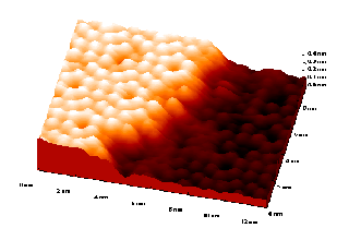
What do we get from
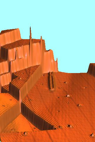
the images? The image on the right is a Silicon surface. We can see a beautiful hexagon shape arrangement to the silicon atoms, which is called the surface structure. This structure can be the same or different to the internal (bulk) structure of the material. Different elements have different structures, for example, most metals have a simple square shape appearing on the surface. The STM is perfect for looking at the structure of the surface but we cannot characterise the atoms. So if there is two metals on the surface it is difficult to distinguish between them. Other important information from the surface images includes growth of atoms as shown below. The image is copper (from IBM) and shows large islands terraces, and steps, which all combine to provide important information classifying surfaces of different species and different combinations of atoms on the surface. |
 |
|
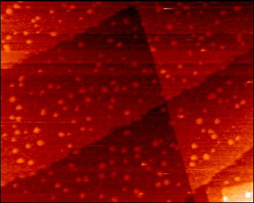
It was concluded that sulphur impurities are segregating to the surface and causing the observed triangular pattern with the sulphur visualised at an origin for step edge growth. Other impurities can be seen on the surface, at point along several step edges. These contaminates could either be from normal segregation from the bulk, adsorption of gas molecule from vacuum or sulphur atoms that have initiated the triangular pattern and diffused across the surface. |
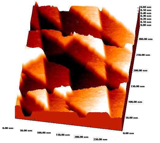
I have investigated the interaction of different environment on a Pd(100) surface. Depending on what temperature the Pd(100) surface is raised, the structure and composition can be altered. Shown below is an example of this for Pd(100) heated up to 950K which displays a distinct triangle pattern on the surface. There is also similarities between this image and the image on the left of the copper surface from IBM. Both images show double steps at the apex of the triangles.
|
 |
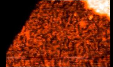
Other patterns that form on the surface of Pd(100) are shown below and on the left. The pattern on the left is from oxygen forming islands on the surface, an unusual occurence for a gas molecule. Below is the formation of a brain-like structure called veins of carbon that segregate to the surface.
|