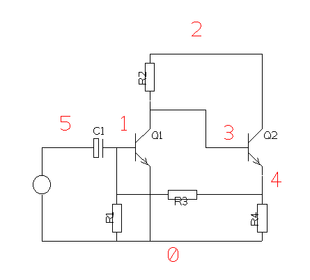
Direct-coupled feedback pair amplifier design
Very few textbooks give an analysis of this amplifier circuit, although it’s very useful. The numbers in red are the nodes for a SPICE simulation.
The following design technique works quite well, gives reasonable results and is very easy to apply.
We need to make a couple of assumptions about the transistors that we are going to use. Let them both have a beta of 200 at a collector current of 1 mA. This enables us to fix the collector current (Ic) of both Q1 and Q2 at 1 mA, so we don’t have to mess about finding the beta for a different Ic.
Assume a supply voltage of 9 V.
For maximum signal handling capability, we need the emitter of Q2 to be about half the supply voltage, 4.5 V. We can now calculate the value of R4, as we know the voltage across it and the current flowing through it:
R4 = 4.5 V/1 mA = 4500 Ohms
With the emitter of Q2 at 4.5 V, the base voltage must be the emitter voltage plus about 0.6 V, say 5.1 V. R2 can now be calculated:
R2 = (9-5.1) V/1 mA = 3900 Ohms
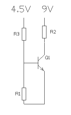
To calculate the values of R1 and R3, we remove Q2 and its associated components, ending up with the simple circuit above. Using the rule of thumb that the current through the voltage divider R3/R1 should be 10 times the base current of Q1 which is 1 mA/200 or 5 uA, we get the following values for R3 and R1:
R3 = (4.5-0.6)V/50uA = 78K
R1 = 0.6V/50uA = 12K
We’ve now got all the values we need to establish the DC conditions of the circuit, and it should work. Let’s check our calculations using the SPICE simulator. The input file for our SPICE analysis looks like this:
DC FEEDBACK PAIR

VCC 2 0 DC 9
VIN 5 0 ac 0.01

R1 1 0 12K
R2 2 3 3.9K
R3 1 4 78K
R4 4 0 4.5K
C1 5 1 10UF

Q1 3 1 0 npn-trans
Q2 2 3 4 npn-trans
.model npn-trans npn (is=2e-15 bf=200 vaf=200)

.op
.end
Running SPICE on this file gave a value of 5.4 V for node 4, quite close to our design value of 4.5 V. Changing the transistor beta to 300 didn’t change it much. Even with beta at 400, it was still 5.3 V, showing that the design can cope with wide variations in transistor parameters.
The foregoing design technique and simulation are very simplistic, but quite adequate for amateur use.