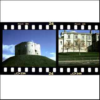
(I am using Valeriy Mikheew�s SCAN.EXE that you can find on Steve Beet's page)
It's an old Mamiya C220 TLR and the sun is ahead so contrast is not that good...
I have had Olympus ES-10 film scanner (parallel port version) for a long time but since I've got Nikon LS-30 I haven't used it at all. Recently I've decided to put it into some use. Say scan 6x6 medium format negatives and slides.
I am pretty easy with putting electronics apart to modify and improve and been inside ES-10 many times before. Its mechanics and electronics is of high quality however some details might be better. Focusing subsystem for example.
Anyway I have removed front assembly with cold light lamp, put a jumper on PCB so that it would not complain about missing film adapter, dismounted lens and CCD line sensor. I have found that cold lamp uses light green filter. I guess its main use is to balance colour negative's mask but what about transparencies then?! Well, Olympus possibly sacrificed slides to colour negative films. It is definitely more popular with amateur photographers this scanner was targeted at...
As to schematic, CCD sensor is connected to ADCs on main board via emitter followers, resistor divider's pots and decoupling capacitors (close to ADC). It's so easy to follow Sony's datasheet without using some thinking... Sony ILX522K CCD sensor's output impedance is only 150 Ohms - low enough to drive any ADC's input directly. Signal frequency bandwidth on this output is around few megahertz and this is analogue output, not digital! Emitter followers are useless and pots just decrease dynamic range of output signal. The only use they were intended for was colour balance calibration instead of doing it by adjusting ADC's reference levels. Bad design of otherwise good thing.
So I have removed transistors and adjustment pots altogether. CCD sensor outputs go directly to ADC inputs via decoupling caps. I have tried to use voltage followers on OPA2604 and AD826 opamps but it did not provide and quality increase. Well, the simpler the better.
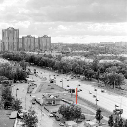
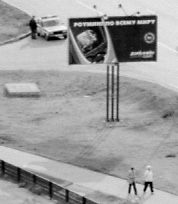
Optical system has to be discarded as it was intended for 1:1 scanning - the lamp and lens moves together with CCD sensor. What it now requires is uniform film lighting and fixed lens that makes 2.5:1 scaled down image that CCD moves across. I made a prototype using medium format 6x7 enlarger. CCD is still mounted on its moving plastic carriage but now facing upwards and what is left from ES-10 is placed on enlarger's projection board. Light isolation is the key so the whole set should be light tight otherwise blacks are loosing details.
Well those are first test scans I have made with it:
(I am using Valeriy Mikheew�s SCAN.EXE that you can find on Steve Beet's page)
It's an old Mamiya C220 TLR and the sun is ahead so contrast is not that good...
And this ES-10 can still scan transparencies:
While looking at CCD sensor datasheet I have realised that its output voltage is linear function of exposure received. With fixed exposure time that means that voltage is linear function of light intensity. Why linear and not simply proportional? Because (1) CCD sensor in a complete darkness produces a black level voltage as high as 5.4V and (2) with receiving more and more light its output voltage decreases until it hits a light saturation level of 3V effectively giving about 2.4V swing between darkness and flooding light.
To add a complexity, Red Green and Blue pixels have different sensitivity to what we see as a white light: their respective sensitivity is 1.86:2.32:1.00. That means that Red pixels reach saturation level almost twice faster then Blue ones let alone Green. However Red and Blue pixels are interleaved on one linear array and Greens are on the separate one and we can control exposure times for R/B and G arrays separately. This is why there are two exposure times in ES-10.
I have to stress again that output saturation caused by too much light is a natural property of CCD sensor. The only way to control it is to vary exposure time or light source intensity. If CCD saturates there is no way to restore lost information in slide's highlights or negative shadows however good following scanner hardware is or how many bits ADC have.
On the other side we do not want to waste sensor's output range because each CCD have relatively high noise level (by the way strongly related to its temperature). As the output swing decreases the signal to noise ratio gets worse and when we finally restore useful information it contains higher amount of noise - it is especially obvious in dark areas of the slide (or negative highlights).
Now we arrive at the first rule of thumb. Exposure (through time or light source) should be set as high as possible and limited only by CCD saturation level. There are two natural limits to choose from: it may be either clear area of film or no film in film carrier at all. First is better but film-type dependant, second is universal but wastes substantial amount of sensor's output (range between clear film base and unobstructed direct lighting). B&W clear film base plus fog transmits only about 40% of light and slide about 70%. If you remember, CCD output is linear, therefore reference to direct light (no film in carrier) may waste 30% - 60% of useful range and result in 1.4-2.5 times increase in image noise level and also cutting down effective image range by 1 bit if ADC reference levels are set to produce 0 for black and 255 for maximum intensity.
However ADCs that are designed specifically to deal with CCD outputs have some useful inbuilt features. First is adjustable levels for reference black and white. They are referred by Vmin and Vplus by Olympus and are adjustable from SCAN.EXE or debug mode in drivers. Vplus refers to darkest level that produces 00 output and Vmin to brightest resulting in 255. It may be difficult to see why logic is seemingly reversed but remembering that black level is highest in voltage and white is lowest it is a bit easier to grasp...