KatipunanBGN© (formerly
KatipunanForum©)
Building a Culture of
Innovation through a Philippine Technology Diaspora
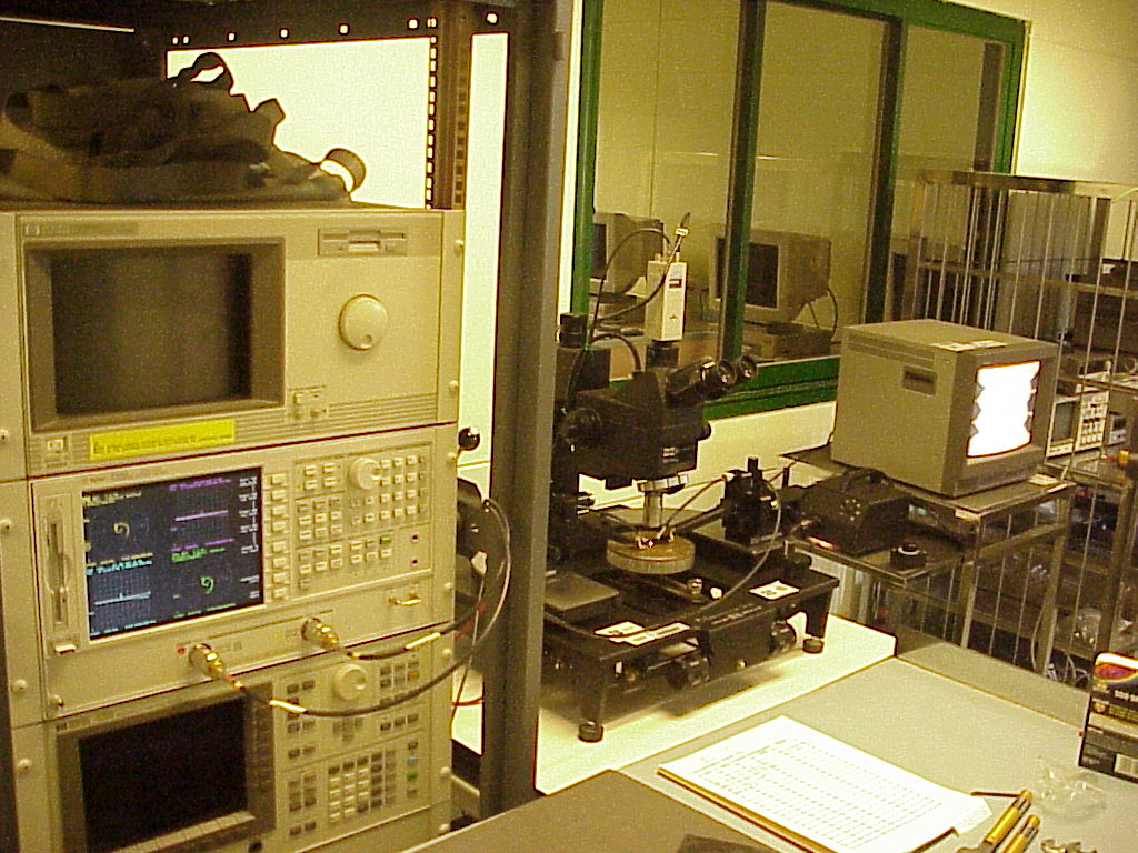
Test rack and wafer prober © UP EEE CAD
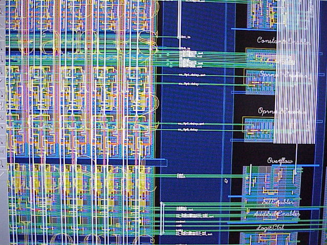
chip layout © UP EEE UP
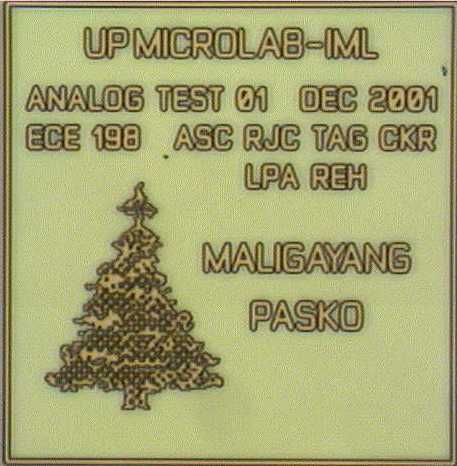
EEE X’mas Tree Run on TSMC 0.25 process © UP EEE
Do We Really Need a (High Volume) Wafer Fab ?
By Dennis Posadas
In
the early days of the chip industry, the battlecry
was “Real Men Have Fabs”. Nowadays, with every
country in
“In Shanghai alone, plans have been announced for about a dozen plants
that by 2005 will be capable of making a half-million wafers a month….Like
CSMC, many of them are foundries, or plants dedicated to contract
manufacturing--an industry pioneered by Taiwan Semiconductor Manufacturing Co.
(TSMC ). Other big plants are in the works in
In
other words, if its cheaper to rent something, why build it ?
Of course, I am oversimplifying the situation here, but if you have a situation
where you have ten or more wafer fabs trying to outdo
each other in a price war, why join them ? Wouldn’t it
be better to work the situation to your advantage ?
“TSMC accounted for half of that volume, and Chang predicts that Taiwanese foundries will
process 40% of the world's wafers by 2010. Meanwhile, hoping to emulate
Which brings me to my second point. While it may not be a good idea to build a volume
manufacturing wafer fab here in the Philippines (from a business perspective,
if the assumptions above hold true), it is definitely a good idea to put our
money in building up the chip design capability AND to setup a university prototype/training
wafer fab facility.
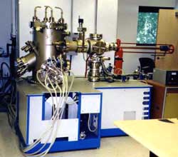
Photo of a Riber EVA32 wafer fab MBE machine similar to the machine donated by the World
Bank to the UP National Institute of Physics
for growing GaAs,
SiGe, InP devices and other
compound semiconductors. The process is scalable to larger production versions
of this machine.
Photo © Riber
Corporation
Now
before we worry about the costs of setting up even a prototype/training wafer fab facility, because of the glut in the world economy, we
actually have a situation where it is a buyer’s market out there for fab
equipment. If ever there was a time to setup a prototype/training wafer fab, it
is NOW. Firesales and bankruptcies are going on in
the developing countries, with equipment going for unheard of prices.
The current and severe IC downturn has put enormous pressure on semiconductor
makers to cut their manufacturing costs--a trend that has propelled the used or
secondary fab-equipment markets, especially in
The used chip-equipment market has been around for years. To complement
their tool procurement efforts, semiconductor makers, IC-packaging providers,
and chip-testing houses over the years have procured a range of low-cost, used
fab equipment from third-party companies, brokers, and even Web-based auction
sites. (
For
those who would argue that all we need is the chip design capability, and our
value added is just to sell the design, that is actually just skimming the
surface. While there are customers for that sort of work, most people look for
a product (and someone to blame for that product). In short, most people want
the actual part, not just the design. What we should aim for are fabless chip companies with niche products, not just pure
design companies. This is where the training fab comes in. We can get
away with utilizing the contract fab foundries, but
if we don’t have a training fab, our relationships w/the contract foundries
might not be productive. We can
insure that our design engineers at least know how a fab works, therefore
allowing them to design better products. We will also be training the people
who need to deal with the customers and the fabs, the
failure analysis and the chip marketing folks.
Now
before anyone argues that these older generation fab equipment are already useless, consider this. You can
actually run MEMS on older equipment such as those used for 6” wafers. And a
lot of these used but perfectly good equipment are
sitting out there at rock bottom prices. Get the picture ?
Just
in case you didn’t know, here is some good news. The University of the
Philippines EEE Department has been training their students to design chips for
some time now. With a corporate sponsored Microelectronics Lab, these students
are already sending their designs for fabrication at TSMC in
In
order for us to play in the higher value added arena of semiconductors and
electronics, we need to have chip design startups from these university
training programs, and invest in at least one local prototype/training wafer fab facility. We can cycle engineers and technicians
through this training fab facility, so that if our local upstarts have any
yield problems dealing with the contract manufacturing fabs,
they would know how to handle it – even if they have to fly off to these
neighboring fabs a few hours away. In short, we
need a prototype/training wafer fab to be able to
take advantage of the excess fab capacity in the
region, not because we want to have our own high volume wafer fab.
The
Diliman-Katipunan area (see separate feature) is a
good place to start. We already have some equipment and expertise we can use as
a base to start a “Silicon Alley”, one that we can position against
Finally, the VC community and the government should
recognize the strategic shift and advantage that would
happen if we have a strong chip design community, with access to a training fab
and trained technicians. We can hold our own even WITHOUT our own volume
manufacturing wafer fab, as we would be surrounded by wafer fabs
in the region trying to insure their own survival, most of them only an hour or
two away by plane.
DISCLAIMER : All KatipunanBGN messages are the
**personal** opinions of the email sender, and do not reflect in any way the
official stance of the corporation, or institution with which the email sender
is connected, or KatipunanBGN. KatipunanBGN is simply an open forum for the
exchange of ideas which will contribute to the development of the