|
|
|
|
         
|
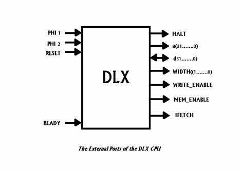
Introduction: The DLX processor was defined by Hennessy and Patterson in as an hypothetical RISC machine with a simple 32-bit load/store architecture. (We have Designed 8 bit Version of Original DLX RISC Processor) This processor is well suited for teaching purposes because of its simple instruction set, its single addressing mode, the simple decoding of its instruction set, and its easy understandable architecture. However, this architecture demonstrates all the major features of the RISC principle. The instruction set of the DLX contains, among others, instructions for signed and unsigned integer arithmetic and for floating point arithmetic. For this design course, only a subset of the original instruction set will be implemented. On the other hand, our processor model is extended by some features: interrupt- and exception handling, three different operation modes (supervisor, user, error), and one additional addressing mode. A pipeline has not yet been included. DLX External Interface: The external interface of the DLX is shown in figure. The DLX has an address bus (ADDR) and a bidirectional data bus (DATA), both 8 bits wide. The output lines RW, ENABLE, and READY are needed to handle the memory access The DLX has an asynchronous reset input (RESET) and a disable input (HALT). A two phase, non-overlapping clock signal is expected at the clock inputs PHI1 and PHI2. The ERROR output indicates to the outside world that the processor has reached an unrecoverable error state. A DLX word is 8 bits long. Memory is byte addressable with a 8-bit address in “Big Endian“ mode, i.e. the byte with the binary address bin“x...x00“ is in the most significant position („big end“) of a 8-bit word .All memory references are through loads and stores between memory and the general-purpose registers. Accesses can be to byte, to a half word, or to word. In the case of half access the address must be „half-aligned“, i.e. the least significant address bit must be 0, in the case of word access the address must be „word-aligned“, i.e. the two least significant address bits must be 0. All instructions are 8 bits wide and must be word-aligned. Reset: An activation of the RESET-input (high active) of the DLXS changes the port direction of the bidirectional data-bus DATA to input and the outputs ENABLE and RW are set to zero. Halt: Before fetching an instruction, the DLX processor checks each time the HALT input. If this input is active, the processor changes to the inactive state. All output ports are set to high impedance state and the DATA bus is switched to input. The processor stays inactive until the HALT signal is set back to zero, and continues afterwards with the normal instruction fetch. Error: In case of a detection of an error, the processor stops any further operation and changes to the error state .This is indicated by setting the output ERROR to one. All output ports are set to high impedance state
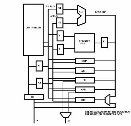
DLX Register Transfer Level Model: We now turn our attention to next level of refinement of our DLX CPU model, a register transfer level description. At this level, The CPU composed of registers, buses, multiplexers , an ALU and a sequential controller.
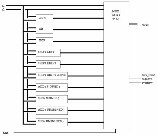
Figure shows register transfer level model of DLX CPU upon which we base our VHDL model. It includes a register file for the general purpose registers ,individual registers for temporary storage (temp) etc. These all corresponds to variable defined in the behavioral architecture of CPU. The Register Transfer Level Model also consists of number of additional registers. The A and B registers are used to store values read from the register file, and the C register stores a result to be written into the register file. The S1 and S2 registers store the two source operands to be operated upon by the arithmetic and logical unit (ALU). The multiplexers At the MDR input allows the MDR to be loaded from the destination bus or the external data bus. The other multiplexer allows memory address to be selected from the PC value or the MAR value. We develop our VHDL description of this implementation by first describing the data path entities and their behavioral architecture bodies. We then use them to construct the register - transfer - level architecture body of the CPU. Finally we describe the behavioral architecture of the controller that sequence data path operation. The Arithmetic and Logic Unit: The ALU in the CPU data path performs the operations on data needed to implement arithmetic and logical instructions. It is also used to perform address arithmetic and to align data for load and store operations. The particular function to be performed by the ALU at any time is determined by the controller. Hence, The ALU must have an input port to select the function.We need to describe the type and allowable values for this port in a separate package, since the type and values need to be accessible both in the ALU description and in the controller description. The entity declaration for ALU consist of generic constant, Tpd, to specify the propagation delay from input to output. The two ports s1 and s2 are the data inputs, and Result is the data output. func port is to selects the function to be performed, and the zero ,negative and Overflow ports are status outputs providing information about the result value.
The registers: The CPU data path makes use of a number of different kinds of registers. The simplest is the flow through latch. The latch consists of input port d and output port q and the control input latch_en. The architecture body consists of concurrent statements. It is sensitive to d and latch_en, since they are the signals included in the waveform and the condition expression. When latch_en is 1 any change on d are copied to the output q. When latch_en is 0,further changes on d are ignored, and the output maintains its previous value. A number of the registers in the CPU data path have one are more outputs that can be disabled from the bus to which they are connected. We us e type dlx_word to implements the buses, so the registers have output ports of this type. Rather than writing different entities for each of the registers with differing numbers of outputs, we write one generic multiple output register. Tpd is the propagation delay. The multiple output registers are used for MAR,PC etc.
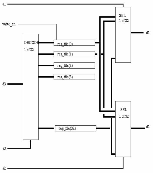
The registry file: The data path diagram shown in rtl organization of DLX CPU includes a register file with two read ports and one write port. The register file must have address inputs to each of these ports. The addresses are determined by the controller, based on the instruction in the IR. At the register-transfer level of modeling, we represent the register address as standard_ logic vectors. The package declaration shown at the top of the dlx_types package defines a subtype for register file address. The subtype is standard_ logic vector, with same index range as the bit_vector type representing register number fields in instructions. The entity declaration for the register file is shown in the program REGFILE . The generic constant Tac represents the access time for reading a word from the register file. Ports q1 and q2 are the two read ports , and d3 is write port. Ports a1,a2, a3 are the corresponding register addresses, and write_en is a control input indicating when the write port should store a value into the register The Multiplexer: The DLX CPU data path includes two multiplexers. The generic constant Tpd specifies the propagation delay from the select input (sel) or either data input (i0 or i1) to the data output (y).The architecture body contains a selected signal assignment statement. When select input is 0,input i0 is transmitted to the output; when it is 1,i1 is transmitted to the output The controller: The controller is one which controls all operation DLX CPU. It consist of several control Signals which is mapped to different modules of the DLX CPU. When ever suitable instruction is received by the controller then corresponding control signals are enabled. Tpd_clk_ctrl specifies the delay between a clock edge and a resulting control output change.
|
©Kallya Prashanth Shenoy 2000
This site was last updated 07/14/02