1. Introduction.
The university has been using the 68000 range of processors for a number of years, however the 68000 is now almost obsolete. Motorola, the makers of the 68000 have added on and improved on the 68000 through the years since it was first introduced but they have gradually replaced them with the PowerPC range.
The technology in microcontrollers has moved so rapidly from what was available during the time of the 68k. Microcontrollers these days require a lot of time to study, support from the makers and open sources. To develop efficient and working code in as little time as possible, powerful development tools have to be used as an aid. These tools allow the developer to see how the microcontroller responds and solve problems before commissioning the product.
The project started in the
summer, suitable development boards had to be found. The requirement of the
University was that the microcontroller development board had to be relatively
cheap and well specified. The University had some software from a company
called Metrowerks® and were interested in using the software for
C/C++ programming as well as assembly language.
After contact with the company,
Axiom’s PB - 555 board was recommended and purchased along with the latest
version of Metrowerks’ software for embedded PowerPC.
1.1
Objectives of the project.
The first guise of this project was a kind of research into the MPC555 and the development environment. After consultation with the supervisor it was decided that the best way to illustrate the operation of this microcontroller was to find a suitable application.
Therefore the first aim of this project is to research and commission a PowerPC® 555 processor and Codewarrior® Integrated development environment (IDE). Commissioning means getting all software needed running on the Host computer, getting the Host PC to communicate with the board and generally sorting out all the teething problems that arise with a new system. This was not very easy as first thought and the reasons why will be explained later in this report.
The research part must be written as a kind of educational guide that will be used by the supervisor and future students on the Masters course. This part of the report is a simple how – to – use guide on the MPC555 and the Codewarrior IDE. It also provides simple programs that allow the user to experience simple programming and debugging first hand. The basic problems have been tackled and the solutions provided.
The next aim of the project was
to develop an application for the MPC555. This will demonstrate that enough
information was gathered during the time of this project to solve a real
problem. The chosen subject area was engine control. This is an area that the
university is very interested in and researched on. The aim of this part of the
project was to use the microcontroller as an engine control unit (ECU). This
means that the microcontroller controls the fuel injection and the spark
ignition of an engine. The target engine was a single cylinder, four stroke
engine called the “
The report will be split into three parts, a section on the microcontroller unit (MCU), one on development and related software and, the last part on the ECU.
2. Background.
The readers of this report must have a basic knowledge of Windows and have a basic knowledge of computers. The report has a brief explanation on engine theory but readers should have an idea how an engine works.
Here are a few facts that may be
interesting.
·
One of the 1st engine management systems
in cars during the 80’s used one Motorola 68HC11 to control ignition. [13]
·
The 68HC11 today is only one of the
microcontrollers in a car. In some cars it is only used to control the power
windows. [13]
·
The timer processor unit can process as much as 28
million instructions per second without main CPU intervention! [13]
·
An average car has about 15 processors; the 1999
Mercedes S-class car has 63 microprocessors while the 1999 BMW has 65
processors!
·
An average car has more processing power sitting
in it than the Apollo missions to the moon! Imagine that.[13]
· Engine management systems are getting faster, more efficient and functional. They will eventually integrate DSP, floating point maths for applications like collision avoidance, electronic stability and emission improvement.
· Engine management units have made modern cars cleaner and increased performance when compared with cars from the 70’s.
3. Hardware
guide.
The PB-0555 is a development
board with I/O pin headers, Debugging ports and RS 232 port. Debugging is done
by a wiggler which connects to the BDM port. Features are [9]:
·
RISC MCU Central Processing Unit (RCPU). 40MHz
operation including floating point unit.
·
Four-Bank Memory Controller
·
U-Bus System Interface Unit (USIU)
·
Flexible Memory Protection Unit
·
448 Kbytes of CDR MoneT Flash EEPROM Memory
(CMF)
·
26 Kbytes of Static RAM
·
General-Purpose I/O Support
·
Two Time Processor Units (TPU3)
·
18-Channel Modular I/O System (MIOS1)
·
Two Queued Analogue-to-Digital Converter Modules
(QADC)
·
Two CAN 2.0B Controller Modules (TouCANs)
·
Queued Serial Multi-Channel Module (QSMCM)
One transistor cell flash technology is used on the MPC555 which
improves the speed and reduces the size needed. The Flash has also been
designed to use 5V for programming, this eliminates the need for an additional
higher voltage power supply.[7]
The MPC 555 has three timer modules two Time Processing Units (TPU3) one
Modular Input/Output System (MIOS1)and 50 I/O channels These provide hardware
timer channels that monitor external events with minimal intervention from the
CPU
The TPU3 is a co-processor with a 32-bit microRISC engine. The TPU has a
micro – engine block that uses 32-bit microcode instructions and is capable of
processing 20 million instructions per second. All instructions are executed in
2 clock cycles. Each TPU3 has 4kbytes of internal ROM that contains predefined
general purpose timing functions and SRAM which can be used to store user
defined functions. An assembler can be found on the Motorola website which
allows code to be written for the TPU.
Some of the functions of the TPU include output compare, pulse width
modulation (PWM), input capture, frequency measurement, missing tooth detection
and frequency measurement. The two TPU3’s can be used to create custom complex
waveforms such as injection and ignition without any external hardware.[2]
The other I/O module is the MIOS1 which is a modular timer system with
both timer and I/O channels. It has 18 timer channels, composed of 10 dual
action channels and 8 PWM channels, and 16 discrete I/O pins. The PWM channels
support high speed PWMs and a resolution of up to 16 bits. They are double
buffered for glitch-free operation and can generate frequencies of up to 10MHz.
They have six selectable operating modes: pulse width measurement, period
measurement, PWM generation, input capture, output compare and discrete I/O.
To provide the A/D requirements of the automotive sensor, the MPC555 has
two 16-channel, 10-bit, Queued Analogue to Digital Converters (QADC). Each QADC
can automatically control up to four external analogue multiplexers allowing a
maximum of 41 input channels. With two QADC modules, the MPC555 therefore can
have up to 82 analogue input channels. Each QADC has 64 result registers that
not only allow the user to obtain the results from all the channels, but also
to make repeated multiple measurements on one channel. Two queues control the
conversion order of the QADC channels. An external event, a software request or
the QADC’s internal periodic timer can trigger the queues to start conversions.[7]
Another module on the MPC555 is the CAN2.0B module. CAN is useful in the
automotive industry because it reduces wiring costs by allowing
microcontrollers from each unit in the car to send data to the engine
management unit. Each message has an identifier which can also deal with
priority. This means all messages can be sent on a single bus.
The MPC555 also includes the Serial communications interface (SCI) that
allows the easy download of information to and from the microcontroller. This
can be used to send debugging information and reduces any external hardware.
4. Development Environment guide
The board was shipped with a PB-0555 development board, Metrowerks Codewarrior for Embedded PowerPC version 6 and a debugging device called the wiggler.
All the software come on CDs and the first step is to install the Codewarrior software. This is done automatically by clicking install when the CD is inserted on the computer. If installing on an NT machine the user must have administrative privileges. The next step is to install the Axiom utility software which contains a simple flash utility.
After installing the Axiom software, the board has to be connected to the host computer. There are two ways which this can be achieved by parallel or serial connection. The Axiom software communicates with the board via the serial port while Codewarrior communicates by either. The device used for the parallel communication is the wiggler which connects to the BDM port of the board.
When using the wiggler the BIOS setting of the PC parallel port mode must be EPP, SPP or bi – directional. The wiggler will not work in ECP mode.
Before any work can be done using Codewarrior, the user has to have a licence key. None of the plug – ins will work without the licence key. To get a licence key, the user has to fill in the registration form which is on the CD or use the MWRegistration program found in the Codewarrior directory. This must be completed and emailed to [email protected]. However it says nothing in the Codewarrior documentation about needing a licence key.
It normally takes about two days for the registration file to be processed. The licence key must be copied using the Edit\Copy button in Windows. The next thing to do is open up the licence.dat found in the C:\...\Metrowerks\Codewarrior directory. This can be opened by using an editor like Word or WordPad. The licence key should then be pasted in this file using the Edit\Paste utility found in Windows. This file must be saved before exiting. The IDE is now ready to be used.
Codewarrior uses the disk serial number in the licence key. If the PC is connected to a network using a network adapter card, the network ID could be used as well. This means the software might not work properly if things are altered.
This section explains how to set up the IDE for use with the board, and how to use the programming tools.
Start Codewarrior either by double clicking on the Icon or from within the start/programs/CodewarriorEPPC6.0 group. The IDE window that is shown in figure 1 below appears. Two types of new projects can be created, an empty project or one with stationary. A project with stationary is one which contains pre - written or precompiled code and libraries. The example code that displays “Hello World” is one such type of file. However most of these are written for general purpose and contain code that is not needed or never used. Most stationary code is also configured for a specific kind of board. However with Codewarrior for EPPC version 6, the Axiom board was not supported. The update of version 6 supports the Axiom board but it was released in April 2002. Subsequent updates will be available from www.metrowerks.com\downloads.
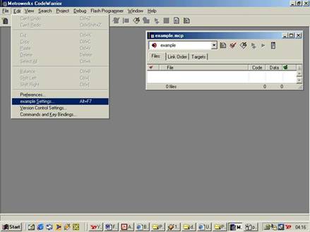
Figure 1. Codewarrior Project window.
A project is a place where all relevant source files and libraries are
found [6]. The IDE opens a project
as a .MCP extension (Metrowerks
CodeWarrior Project).
A project can be opened in the main menu by selecting the File\New option. The projects in this report use the Empty projects option. After selecting the project name and directory, the Project window appears. The project is controlled from here. Source files can be added or removed, assembled, linked, flashed, and tested from the project window. The user must get Codewarrior to work with the target board. This is referred to as a remote connection. Selecting the Edit\Preferences option will bring up the IDE preferences window. Expanding the Debugger option reveals the remote connection options. In the remote connection window the type of connection must be specified. The Macraigor wiggler is used to connect with the board, select MSI wiggler and click the change button. Another window pops up and in connection type: choose parallel , Parallel port:LPT1, speed should be left at one. When done, click the apply button.
The next thing to set up is the
target. A target is defined as the final destination of any output from the
IDE. This means that the type of processor must be defined, the options
required, memory and information needed to debug. This allows the IDE to
download the correct type of code for a particular processor to the right place
and monitor all requested events. This can be done in the target settings
panel. Initially, target is the name of the project. Choose Edit\Target
settings. The target name can be changed to for example RAM or Flash. And the
linker must be changed to PowerPC EABI. This automatically changes the rest of
the other settings in the target settings panels. The linker choice affects the
visibility of other related panels so it must be set before target-specific options like compiler and linker
settings.
The next important thing to set up is the target processor. This tells the assembler what type of code to generate. This is achieved by expanding the Code generation tab in the target settings panel and selecting target processor.
The linker setting tells the compiler where to put the code and debugging information. The linker is an EABI linker. EABI stands for Embedded Application binary Interface. The EABI is a set of conventions for embedded applications and development tools designed to ensure compatibility. It provides software developers the opportunity to choose among various vendors of compiled libraries and software development tools. As long as they are EABI compliant, they will work correctly with each other [6]. The linker panel defines the stack address and the origin of the code and data sections. It also provides the programmer with a tool called a Link map which is a visual representation of how the code is mapped into memory. Care must be taken to specify that the linker does not try and overwrite the memory allocated to the AxIDE monitor software on the board. If this does happen, the flash utility will not write the code. An alternative way is to use a linker command file which will be covered later in this document, this option can be selected by checking the linker command file box. If a linker command file is not used files are linked in the order that they are arranged in the link order of the project window.
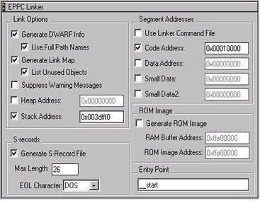
Figure 2 Linker Panel in Target settings
The debugger allows selected events to be monitored on the IDE for example exceptions. This also has to be set up according to the processor. The debugger needs to know the start of the executable. After the code was compiled / linked an executable was generated with a .ELF extension. The board also needs to be “initialised” every time a program is executed. Initialisation sets the state of the microcontroller like the clock speed, Interrupt masking, oscillator selection, privilege, etc. These are controlled by some registers and the values to be assigned to these registers could be stored in an initialisation file. This option should be selected when running the program from RAM and BDM. Some examples of initialisation files can be found in C:\...\PowerPC_EABI _Support\Initialisation_files directory.
4.4 Program writing.
To start writing source code, click the new
text file icon on the menu or file\new\file and select text file. After writing
the source code it must be saved as .ASM, .C or .CPP. The compiler /assembler
for each type of code were automatically set up when the EABI linker was
selected. The project must be saved before it can be added to a project. This
can be done by choosing the project \ add files in the menu bar. All the code
in this report was written in assembly language. Some things are necessary for
assembler code they are called assembler directives. They tell the assembler
how to arrange the code and must be included in the source files.
The basic things to note are [12]:
The .text directive: This tells the code section that follows is executable code. This must always be in front of code in a file
The .data directive: Specifies an initialized read-write data
section. This part of code is normally copied to RAM when program execution
starts
The .rodata directive: Specifies an initialized read-only data
section. This is useful if some kind of protection is needed.
The .equ directive: This assigns a numerical value to a particular
string. For example Ram . equ 0x3fa000. The “=” signs also does the same
function.
The .section directive: Defines a section in an object file. These
files take on addresses specified in the linker command file or start at the
end of the previous section according to the link order.
The syntax for this directive is: .section
name [alignment]
The .ascii and .asciz directives: the assembler will allocate a block of memory for storage for the ascii string defined by these instructions. The assembler will allocate a byte for each character. The .asciz defined string will be zero terminated.
The syntax for the .ascii and .asciz instructions are;
[label] .asci(i)(z) “string”
The .global directive: This tells the assembler to make the file available to be called by other functions.
The .extern directive: This is used as a reference to other files. It tells the assembler to import the file / function defined by the label.
4.5 Compiling and linking code.
Compiling is the process of turning the source file into a format which the target processor recognises called the object code However, this code must reside in a particular location in memory with other object files and binaries like the flash engine. The process of bringing all this together is called linking.
This can be controlled by two methods, the first is the linker panel in the target settings and the second is the linker command file. The first method has been covered. Appendix D is an example of a linker command file.
A linker command file can be created by using a text editor and saving as .lcf. The key directives and instructions are listed below.
The Memory directive.
The memory directive defines the destination of code and must be specified first. It has the following syntax
Memory [<label>: origin = <address> length = <value>]
The label could be ram or rom. Origin is the address of start of the block and length the size in hex.
The Sections directive.
The sections directive is used to define the hierarchy of the code sections and also include absolute addresses where necessary. The syntax is of the form as shown below.
Sections [.section name (type) <address modifier>(address): {}]
Where type is any one of text, data, const or mixed. The address modifier could be BIND or ALIGN. BIND allocates the section to an absolute address while ALIGN aligns the code at the boundaries specified by the hex value.
The GROUP directive.
This specifies what particular group of sections should be put into a defined block of memory. For example
GROUP: {<list of sections>} > ram
The linker command file can only be used if the option is selected in the linker panel.
After all source code have been
written, the project is compiled by selecting the make button ![]() or
pressing F7.
or
pressing F7.
If there are errors, an error and warning window pops up. If successful a .MAP file and a .MOT is created. The .MOT file is the input of the flash programmer.
4.6
Downloading the program to the board.
The code .MOT file must be downloaded to the board before
the compiled code can be executed. Codewarrior has a flash programmer utility,
however there is a target resident programmer on the board. This programmer can
be accessed by clicking on start\programs\AxIDE. This utility will work only if
the PROG_EN jumper is installed, the serial connection on and the wiggler
disconnected. To download the program to flash on the board, option one, the debug
monitor is used. Typing dl causes the monitor program to prompt for the
location of the .MOT file to be flashed. This can be specified by using the
upload button. This is only for when RAM is the target. To execute the code,
type go <start_address>. The contents of memory can also be viewed using
the md <address> command and modified using mm <address>.
If the flash memory is the destination, the 2nd option must be selected which is the On – chip CMF flash programming. The monitor program resides in the first 64k of memory so the code to be flashed must start from 0x10000 onwards. The steps for programming using the AxIDE flash programmer are:
The EX_CFG jumper should be off and VPP_EN and PROG_EN on.
In the utilities menu option 2, CMF flash programmer should be selected.
The user space in the flash memory should be erased by selecting E
Select P to download the program.
The VPP_EN jumper must be removed after programming is finished. This jumper enables the programming voltage.
The program can be tested by selecting T in the menu.
Removing the PROG_EN button allows the program that is located at 0x10100 run at start – up.
After the program has been downloaded advanced debugging can be done using Metrowerks Codewarrior.
4.7. Debugging using Codewarrior.
A debugger controls program execution and shows the internal operation of a computer program. The debugger is used to find problems while the program executes. The debugger is also used to observe how a program uses memory and the result of every instruction or task.
The CodeWarrior debugger provides the
following features for the control of a program.
Execution of one instruction at a time
(trace or single stepping)
Pause in execution after a previously set
point is reached in the program. These are known as breakpoints.
Suspension of execution after changing a
specified memory location. These are known as watch points.
The operation of the machine can be monitored using several windows and after a pause in execution the values of a register or memory location can be viewed or altered.
The debugger window has some basic commands like run, stop, kill, step over, step into and step out.
![]()
![]()
![]()
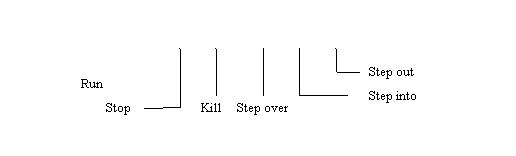
Figure 3 Debugger command panel
· The run button opens up the debug window and also executes the .ELF file. It single steps through the instructions.
· The stop button suspends the running program at any location it might be currently at.
· The kill button terminates the debug session, closes the window and returns the user to the project window.
·
The step over command performs the operation to
the line to which the current statement arrow points![]() . If the
current line is a subroutine call the debugger will execute the subroutine
without single stepping it.
. If the
current line is a subroutine call the debugger will execute the subroutine
without single stepping it.
·
The step in command performs the operation to
the line to which the current statement arrow points![]() . If the
current line is a subroutine call, the debugger branches into the subroutine
allowing the user to see the operation of the subroutine.
. If the
current line is a subroutine call, the debugger branches into the subroutine
allowing the user to see the operation of the subroutine.
· The step out command allows the user to get out of a particular function that is being executed.
A typical debugging session is shown in figure 4 below
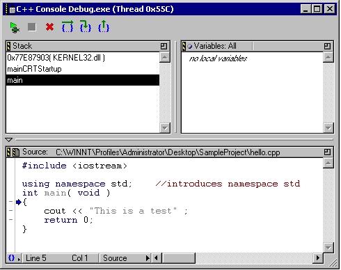
Figure 4 A typical debugging window.
4.6.1 Using breakpoints.
Breakpoints are used to suspend program
execution at a particular line in a source code. This can save a lot of time if
a problem needs to be found in a long program. The program can be executed
until a suspected problem point or line and single stepped there after wards. The program executes statements normally until reaching the
breakpoint. The debugger then halts the program, preventing the line that
contains the breakpoint from executing.
A breakpoint can be set by just clicking on the line desired in the
source code prior to downloading the .ELF file for debugging. A red dot ![]() appears, showing a break point has been set.
Clicking on the line again removes the breakpoint.
appears, showing a break point has been set.
Clicking on the line again removes the breakpoint.
4.6.2 Source code display modes.
The source code display mode can be specified at the bottom of the debugger window. The source display mode displays the C file or the assembler file. The assembler mode displays the assembler file, the addresses and the machine code. While the mixed mode displays both
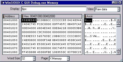
Figure 5 Memory display window
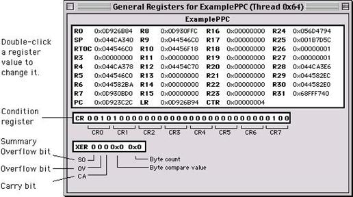
Figure 6 The register display window.
4.8 Conclusion.
This is the end of the section about the development tools. The Codewarrior tool is a powerful tool which can speed up the development process. However there is a small limitation, the inability to run the code and view the registers. That is, without single stepping there is no way to view the registers. This makes debugging programs with interrupts more difficult than it should because the program has to be single stepped to view results.
The documentation too is very poor and there are very few resources available. This is probably due to the high cost of the Codewarrior software which puts off amateur developers. Metrowerks have better documentation for all the other Codewarrior products like MCORE, Java, C++. Almost all the products have an online tutorial group except for EPPC that is.
- Ram_fill.
- Pulse_gen.
- TPU_waves.
The full software listings are available in the appendix.
5.1.1 Ram_fill: A brief description.
One of the limitations of the development board is the lack of visual I/O that can be used to demonstrate a test program for example to write a pattern to a group of LEDs. Ram_fill allows is a simple program that is used to fill a block of RAM with a value. It is simple enough for any one with no experience with microcontrollers to write and understand. It also uses the debugger as a kind of display tool to give assurance that the program works. It fills up RAM locations 0x3fb000 to 0x3fb00f with 0xba. It uses a special purpose register called the count register as loop counter. The results can be seen in Figure 7 below
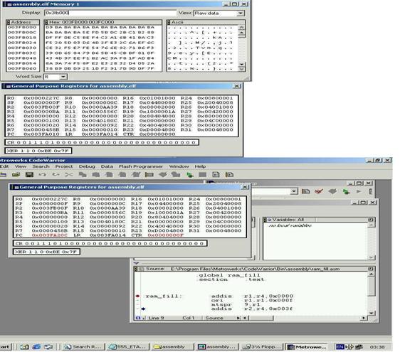
Figure7 Results of Ram_fill (showing affected RAM locations).
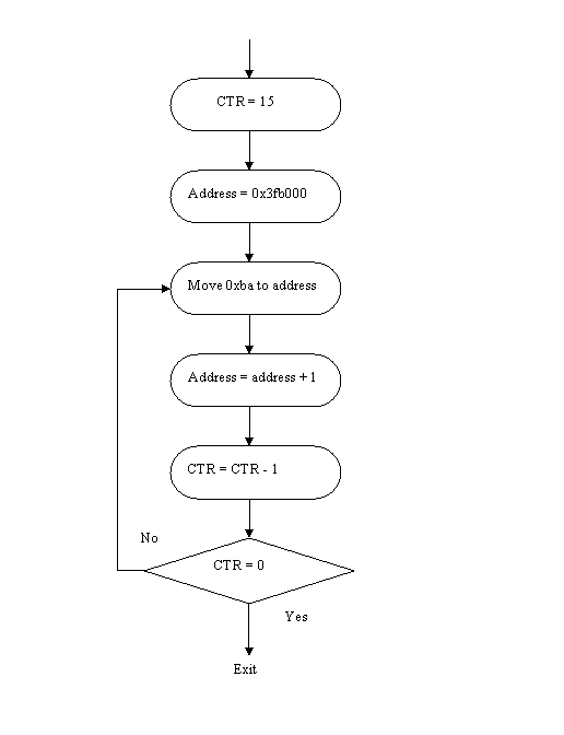
Figure 8 RAM_fill flow chart.
5.1.3 Pulse_Gen: A brief description.
This program uses the PIT to generate periodic pulses. PIT means periodic interrupt timer. It can be set up to generate interrupts between 64 microseconds to 4.19 seconds intervals [3]. This example does not use interrupts however it polls the PIT interrupt status flag. It also uses the Modular input/ output sub module general purpose pins as an output. This example increases familiarity with general purpose I/O, counters, interrupts and the system clocks. This routine generates square waves with a 20ms period.
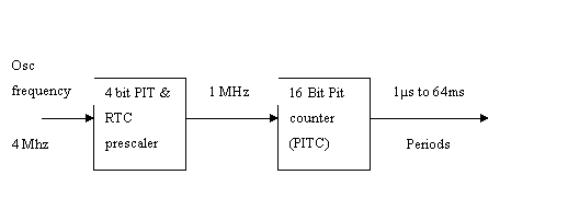
Figure 9 The set up of the PIT
Pulse_Gen flow chart.
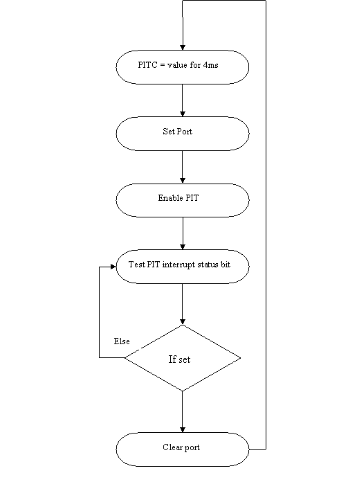
Figure 10
5.1.4 TPU_pulse: A brief description.
This program uses the timer
processing unit to generate pulses. That will be used to simulate the waveforms
for the sensors on the
The TPU matches the timers with
the offsets which were preloaded into the parameter RAM. The value of any of
the offsets must not be greater the 0x7fff because the TPU shifts the values to
the left. When the offset value in the parameter RAM is matched the timer looks
at the associated event of the parameter RAM. This can be output low or output
high and writes that value to the TPU pin data register as can be seen in figure
11. In this way complex waveforms can be made. The normal value of offsets is
five but if channel 14 is used it can be linked with channel 15 to have 14
offsets. The function of the TPU that is being used to generate these waveforms
is Queued output match (
It uses the IMB clock as a timer source for the counter. The IMB clock has been set to match the system clock frequency.
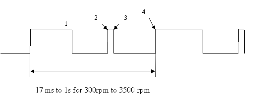
Figure 11 The output of the optical sensor over 720 degrees.
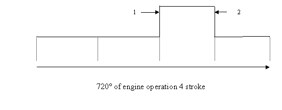
Figure 12 Output from inlet sensor.
The key registers to set are.
UIMB module configuration register UMCR: The value must correspond to full speed.
PLL low power reset and control register: PLPRCR set to desired value 20 or 40 MHZ, though 40MHz is used throughout this project.
TPU module configuration register: TPUMCR set to enable TPU version 3 and divide clock by 8
Channel function select register
CFSR0: channel 12 and 15 for
Host service sequence registers HSQR0: enable the channels for continuous mode.
Host service request registers HSSR0: Initial values of pins
The TPU timer count register is clocked every 10µs.
Section 6: Engine Control Unit.
6.1 The
Engine.
The modern internal combustion engine has not changed much in principle from the first engine produced about 100 years ago. The engine uses the energy derived from igniting gases to generate movement. When a gas is heated it expands and if ignited a large amount of energy can be harnessed. The internal combustion has several hundreds of these explosions per minute taking place in the cylinders.
There are various examples of the
internal combustion engine the most popular being the four stroke or Otto cycle
engine. Some others are two stroke cycle, Wankel engine and the Miller engine.
The four stroke engine was invented by Nicklaus Otto in 1867. The
6.2 The four stroke engine.
The four stroke engine is so called because the operation of the engine can be split into four distinctive stages. These correspond to the movements of the piston between top dead centre (TDC) and bottom dead centre (BDC) for each combustion cycle. The piston rotates through 720 degrees in a complete combustion cycle. The stages in sequential order are:
· The Intake stroke.
· The compression stroke.
· The combustion or power stroke.
· The Exhaust stroke.
6.2.1 The intake stroke.
The intake stroke begins with the
piston near the top dead centre. As the piston begins its descent, the exhaust
valve closes fully, the intake valve opens and the volume of the combustion
chamber begins to increase, creating a vacuum. As the piston descends, an
air/fuel mixture is drawn from the fuel injectors into the cylinder through the
intake manifold. The intake valve closes just after the beginning of the piston
upstroke thus ending the intake stroke. The needed amount of fuel must be
injected at the intake stroke. Figure 13 shows the intake stroke in a cylinder.

Figure13 Intake stroke of a four stroke cycle.
6.2.2 The compression stroke.
As the piston moves up the cylinder from bottom dead centre to top, the air / fuel mixture is forced into the small chamber in the cylinder head. This compresses the mixture until it occupies about 10% of the volume that it did at the beginning of the cycle [10]. This compression raises the temperature of the mixture and increases its pressure, increasing the force generated during the ignition cycle. From the diagram below it can be seen that the fuel / air mixture is quickly and effectively compresses because of the smaller volume at the cylinder head and the compressing action of the piston.

Figure 14 Compression stroke.
6.2.3 Ignition or Power stroke.
The air/fuel mixture is ignited
by the spark plug just before the piston reaches the top dead centre. The heat
produced by combustion increases the pressure in the cylinder, pushing the
piston down with great force (figure15). This is the cycle that actually
creates power in an engine hence the name power stroke. The spark is caused by
discharging the coil connected to the spark plug. The Piston connects to
the crankshaft which turns the translational motion to rotational
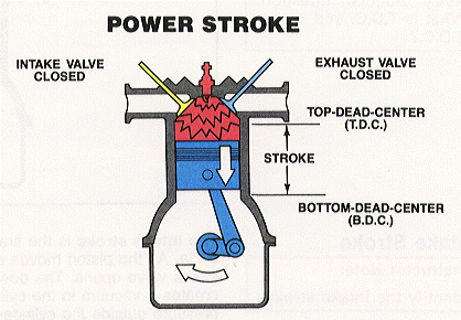
Figure15 The Power stroke.
6.2.4 The exhaust stroke.
As the piston approaches the bottom dead centre, the exhaust valve
begins opening and the pressure in the cylinder begins to force the gasses out through
the valve (Figure16). The ascent of the piston then forces nearly all the rest
of the unburned gasses from the cylinder. The cycle begins again as the exhaust
valve closes, the intake valve opens and the piston begins descending and
bringing a fresh charge of air and fuel into the combustion chamber. This
completes the 4 stroke cycle.

Figure16 The exhaust cycle.
7. Overview of Engine
Management.
The carburettor used to be the primary device for controlling fuel supply in internal combustion engines. The demise of the carburettor was caused by the rocketing fuel crisis of the 1970’s.[13] The carburettor is a mechanical open loop device. A mechanical system is not very accurate or fast as an electronic one. Also for information to be processed mechanical parts had to be used and these slowed engine response and wasted lots of fuel.
The next generation of carburettors were electronic and used fuel injectors. This slightly improved fuel economy because fuel could be delivered more accurately. By this time fuel economy was not the only problem that manufacturers faced, there were growing concerns about emissions and the ozone layer. New emission laws were passed and consumer awareness on this issue increased. It was around this time that catalytic converters were introduced.
Engineers knew that the products of combustion - both power and
pollutants - were affected by how precisely the fuel/air mixture approached
theoretical perfection and when the ignition event took place. To get clean
air, fuel had to be precisely mixed in a "stoichiometric" 14.7:1
ratio [11]. The mixture had to be
ignited at a precise instant that varied with load, speed, and other factors.
Mechanical devices could not achieve the required precision and automakers soon
approached manufacturers of computers and microcontrollers. (A microcomputer
chip with a single pre-programmed task is referred to as a microcontroller.)
Sensors were the solution to the car manufacturers’ problems they provided information on exactly when an event occurred and by how much. This meant that the response could be varied depending on an exact situation instead of implementing a general solution.
7.2 ENGINE CONTROL UNIT.
All cars manufactured today contain at least one microcontroller for the
ignition system. A well-designed ignition system is important to a
vehicle that starts under the worst conditions, idles smoothly, and delivers
the maximum fuel economy while producing low emissions. The ignition system’s
primary function is to produce fuel and spark pulses. The microcontroller is responsible
for the proper timing of the signals that control the fuel and spark within the
engine control system. The
microcontroller receives information from many different sensors, including:
The engine position sensor
Inlet air pressure sensor
The air temperature sensor
The oxygen sensor (lambda)
The air mass flow sensor
Sensor data (voltage, temperature, oxygen content etc.) must be
converted from analogue form into the digital form required by
microcontrollers. This Analogue-to-Digital conversion is typically performed
within the microcontroller.
The ability to capture and compare events as they happen is very
important. High-speed input and output channels transport data to the
microcontroller for action. The microprocessor core itself needs raw power and
speed as it executes the complex instruction codes called algorithms.
Once sensors, algorithms have been finished, control signals are sent
out to tell the engine what to do. High-speed channels specify when and how
long to fire spark plugs, send fuel through the injectors. The unit needs to
know from the sensors the effect of the actions taken.
Information, like parameter values is typically stored in flash memory.
In addition to this, flash is the non - volatile memory of choice for Engine
Control Units for the operating code because it can be updated by mechanics or
repair men.
The algorithms for an engine management unit can be very complex so only
the first two sensors will be used in this project.
8
The Suffolk
The
A disc with one 90 degree slot and a 1 degree slot is attached to the
crankshaft of the engine. Thus, the disc spins at the same speed of the engine.
If the disc is carefully placed it can be used to determine the position of the
engine. This is illustrated in the figure below. The 90 degree slot starts at
29 degrees after TDC and the 1 degree slot starts 19 degrees after BDC [1]
Figure17 Representation of the slotted disc of the engine.
8.2
Sensors of the engine.
The engine has a variety of sensors on it however only two will be used the optosensor and the inlet valve sensor. The operation of the optosensor can be seen in the diagram above. As the engine is spinning the slots of the disc pass underneath the optosensor generates a logic 1for transparent bits and a logic 0 otherwise this make s the output from the optosensor look like figure 11 above.
This output can be fed into one of the microcontroller’s input channels and sampled to determine engine speed and position. The 90 degree slot can be used to determine engine speed by using the formula below
![]() engine speed (rpm) =
engine speed (rpm) = ![]()
The small slot determines when to start the ignition algorithm.
The times for this the 90 degree
slot are from 47.6µs to 2.78 ms while the 90 degree slot ranges from
The inlet valve pressure sensor is the other sensor that will be used in the ECU algorithm it operates over the 720 degree cycle of the engine. The output of the inlet valve is a logic 1 when the inlet valve is open and a logic 0 when the inlet valve is closed it makes sure that the fuel injector injects fuel at the intake stroke and increases fuel economy.
8.3 Operation of the ECU.
The inputs to the engine control unit have been discussed in the section above, they are what the ECU uses to regulate the outputs. This type of system is called closed loop control. The outputs that the ECU will have are
· Fuel Injection.
· Ignition.
8.4 Fuel Ignition system.
The Fuel injection algorithm is starts
at the end of the 90 degree slot. This however will only be carried out if the
inlet valve pressure sensor indicates a logic 1. If the inlet valve pressure
sensor indicates a logic 1, then the fuel will be injected just after the
bottom dead centre. The richness of the fuel / air determines the engine speed,
the richer the mixture the faster the engine will turn. [10]
The value for the amount of fuel to be injected is pre – programmed and can be varied depending on the desired speed.
The output from the injection port is connected to the fuel injection driver circuit. When the injector pulse is applied, the electromagnetic coil attracts the plunger which moves up, allowing pressurised fuel to squirt out through the nozzle [11]. The pressurised fuel is supplied by a fuel rail. The amount of fuel is controlled by the pulse width modulated waves from the injection pin of the microcontroller.
8.5 The ignition system.
The microcontroller starts the ignition process when the small slot is detected the ignition port charges the coil through the ignition port circuit. The coil takes a finite time to charge and this is called the coil charge time (CCT)
The ignition driver circuit consists of an amplifying stage which raises the value to 12 Volts. This value is then passed through a transistor drive circuit to the primary winding of a coil. The magnetic flux induces voltage in the secondary winding and can be as high as 30kV. If the primary voltage is removed the coil discharges creating an electrostatic spark.
9 Design of the ECU.
9.1 Methodology.
The first things to be considered are the inputs and outputs. the inputs are:
· Injection time
· Coil Charge time (CCT)
· Coil charge angle.
· Engine position
· Engine speed
The outputs are;
· Fuel injection
·
Ignition.
The timing of the outputs depends on the sequence at which the inputs happen. Therefore the following must be considered
· The inputs must be accurate to guarantee desired outputs. For instance if the voltage outputs from the sensors are not high enough they might be interpreted as a logic 0.
· One stage must be completed before the next stage. The ECU must be fast enough to detect inputs and process the necessary algorithms. Fuel must be injected in order for ignition to occur.
To meet the requirements the fastest time for the slots, instruction timing and latency, the minimum pulses detected.
The injection pulse width for providing a rich mixture is 4.8ms and the coil charge time is 4.28ms. These times are fixed. They must be subtracted from the total time it takes for the rotating slotted disc to complete one cycle to ensure that the algorithm can be done in time. The minimum time for one revolution is 17ms which leaves a time of a about 8ms for algorithm processing. A clock speed of 40 MHz and an average instruction latency of 1 clock cycle means 320,000 instructions can be processed.
As this project is largely a research project mid- range values were selected to determine if the algorithm will work. An injection time of 2ms, coil charge of 4.28ms, a firing angle of 20 degrees before TDC and a 90 degree offset.
The inputs from the sensors were simulated using the timer processor units (TPU) on board, these provide very accurate pulses and can be varied easily.
The periodic interrupt timer was used as a counter for the generation of the pulse width outputs. The PIT was set up to be clocked internally at a rate of 1µs. This meant that any time between 64µs and 4s could be generated by putting a multiplication factor in the 16 bit PIT counter.
The MPC555 has a double action submodule (MDASM) in the MIOS (modular input / output submodule). The MDASM’ pulse width measurement function put the time of the leading edge and trailing edge in two separate registers and generated an interrupt. Time for one period was the difference between two registers thereby reducing software overhead and CPU processing time when compared to a polling process [5]. Polling means that the CPU keeps looking for a particular interrupt till it occurred. Interrupts mean that the processor is free to do other things until the event occurs. To further reduce the software overhead the MIOS counter and the PITC are clocked at the same rate so that there is no need to convert values when doing the calculations.
9.2 The ECU algorithm.
The MDASM is set up to start when a rising edge is detected and stop operation at a falling edge. At the falling edge an interrupt is generated. On receiving the interrupt, the CPU reads a 32 bit value from the counter. Each counter is 16 bits but to reduce processing time a word read is done because the counters have consecutive addresses. The upper bit is stored in another register and the lower bit masked. The greater value is subtracted from the smaller and compared with the hexadecimal value equivalent to 2ms to determine the slot that caused the interrupt.
If the 90 degree slot caused the interrupt, the time is stored in memory, injection port set and the injection time is loaded into the PITC and the PIT enabled. The injection port is cleared when the PIT interrupt status is detected and the interrupt routine is terminated
If the 1 degree slot caused the
interrupt, the time for 90 degrees is fetched and divided by 90 degrees to get
the time for 1 degree. The reason for doing this is that it improves the
chances of the algorithm working if for some reason the engine goes faster than
3500rpm. The value for the firing angle and the offset are fetched and added to
get the overall desired firing angle. This is multiplied by the time of 1
degree to find how long the spark event is from the small slot. The coil
however takes a finite time to charge and this must be subtracted from the firing
time. Therefore the ignition coil output is always on for 4.28ms.The PIT is
first loaded with the offset time and then the CCT. This process is then
repeated again
9.3 Advantages of using MPC555.
The processor can operate at 40MHz and capable of 52Million instructions per second [13].
Most instructions take one clock cycle even branch instructions. [4]
The timer processor unit can carry out most automotive functions without CPU intervention.
The amount of on – board systems like CAN, QADC, Serial Communication ports and Timers make it easier to send and process information
The double action of the MIOS
means software overhead can be reduced.
ECU algorithm flow chart.
Figure 19
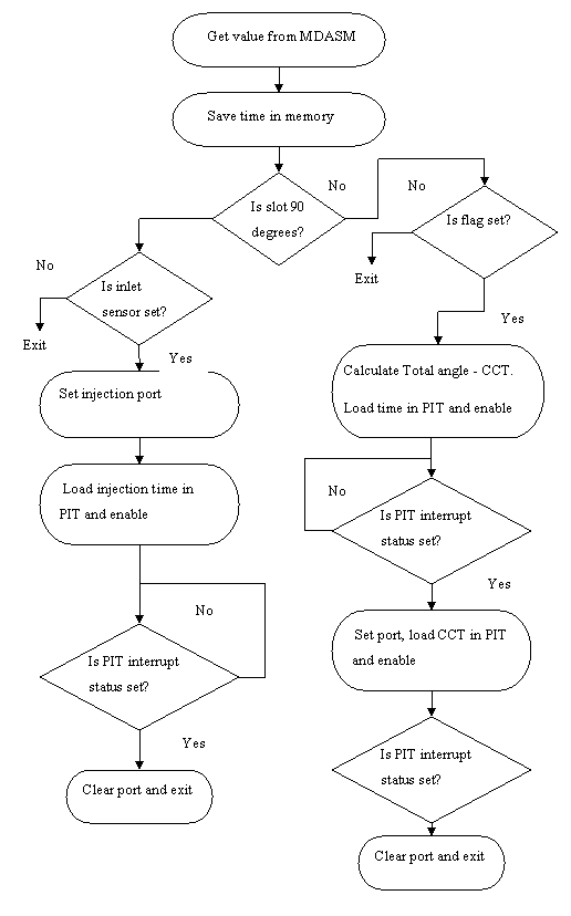
Figure 20
9.3 Limitations of the algorithm.
The whole set up is nothing more than a constant speed regulator. It assumes that the engine speed will be constant if a constant amount of fuel is injected. There are other factors which will influence the speed like the oxygen content. The less the oxygen content the more difficult it is for the mixture to burn.
The algorithm also assume the throttle position will remain constant during it’s operation. If the throttle does open the whole process will fail because the air / fuel mixture will be richer and the inlet sensor have air rush into it even when it is closed.
9.4 Discussion of results.
The results for the ECU were as expected the TPU outputs which generated the inputs to the algorithm were very accurate. The outputs of the TPU were made to mimic what the optosensor and inlet valve output will look like at 2500rpm. The results can be seen below in the pictures.
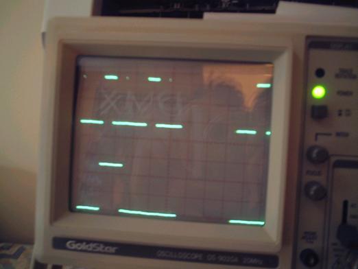
Figure 20.
The Optosensor output is the one on the top. At 2500 rpm the 90 degree slot is 6ms long which is proven in this picture because each division is 5ms. the small slot is 50µs long and can just be made out.
The second wave at the bottom is the inlet sensor wave form. This is shown in figure 21 with the oscilloscope at 2ms per division.
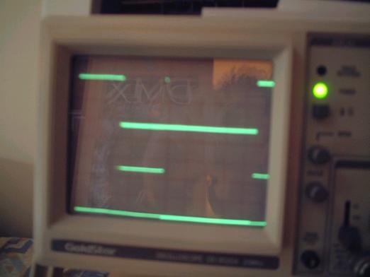
Figure 21 TPU outputs at 5ms per division.
The picture below shows the Ignition port at the top and the fuel injection port at the bottom. The fuel injection port is about 2ms and the CCT is inaccurate at 6ms. The reason for this could not be determined at the time of the report. Altough the timing of the board depended on the time programmed into the clock registers the onboard flash utility and monitor used 20MHz while the ECU used 40MHz. Resetting this register during operation of the ECU caused the clock to lose phase or a reset. The solution will be to change the ECU to use 20 MHz.

Figure 22. The ignition coil output and the injection port output. (2ms per division).
Future developments.
The project could be made to be a proper engine management system by incorporating other sensors. Some of these other sensors could be the oxygen sensor and air mass flow sensor. These sensors have analogue outputs, this will mean that the Analogue to digital converters will have to be used.
Perhaps, a real engine could be controlled in the future which means the outputs have to be connected to proper interfaces. Electrical issues like the current drawn from the pins will have to be considered.
The program also uses a lot of assembly language which take very long to write and more difficult to debug. C or C++ should be used in all future projects except when setting up registers.
The parameters used as inputs are downloaded to the board while programming the chip. To make the project more dynamic, the parameters could be downloaded during run time using the serial communications interface.
The board also has on - board flash utility, this program uses a lot of the internal flash space, future project students could write a new flash algorithm in their programs, that downloads itself.
The board also lacks visual I/O like LED’s, this might prove invaluable for debugging purposes.
All this things were considered during the time of this project but the problems of commissioning the board meant other things had to be done first.
Conclusions.
All the objectives of the project were achieved. The research part of the project took the longest. There were too many problems in commissioning the project Poor documentation and long response times were the reason for this. Also the PowerPC processor is very much difficult than microcontrollers studied previously on the course. Nevertheless, the guide written on the development tools covers most of the aspects.
The engine control bit of the project was also considered to be successful because the project uses the simulated inputs to give reasonable outputs even though the engine was not used. The only problem was the Ignition outputs all others behaved as expected.
The PowerPC architecture is very widely used, doing this project has increased my portfolio of embedded systems design. Thee microcontroller is also very modern and knowledge gained from this project can be used in designing DSP systems, real time applications, not to mention engine management.
References.
· [1] Engine management unit for a single cylinder four stroke test engine by Dionysis Alevizakis
· [2] TPU Time processing unit reference manual TPURM/AD revision 3 by Motorola.
· [3] MPC555 Interrupts AN2109/D application note by John Dunlop and Steve Mihalik Rev 0.26.
· [4] RCPU reference manual RCPURM/AD by Motorola.
· [5] Using the MPC555 as a frequency counter – Motorola application note AN1778 by Motorola
·
[6] Queued output match TPU function (
· [7] MPC555 / 556 users manual – Motorola 2000.
· [8] Targeting embedded PowerPC Systems. PDF user’s guide for Codewarrior. Published by Metrowerks.
· [9] PB - 0555-A Motorola MPC555 PowerPC Microcontroller Board. Development Board manual. Published by Axiom manufacturing.
· [10] Introduction to Internal Combustion Engines. By Richard Stone, Third Edition. Macmillan 1999
· [11] Automotive electronic systems. By Trevor Mellard – Heinemman 1987.
· [12] Assembler Reference guide. PDF document published by Metrowerks.
· [13]. http://e-www.motorola.com/collateral/ENGINECONTROLART.pdf - white paper published by Motorola on eengine management.
Bibliography.
·
C by Dissection – The Essentials of C
programming. Second edition. – By Al Kelley and Ira Pohl. Benjamins / Cummins
Publishing 1992
·
MPC500 System Integration Unit Reference Manual
(SIURM/AD) – Published by Motorola.
·
IDE user’s guide – PDF document on how to use codewarrior – Published by Metrowerks.
·
The Zen of BDM – Whitepaper on debugging by
Craig Haller of Macraigor Systems. http://www.metrowerks.com/tools/documentation/embedded/zenofbdm/
URL’s.
·
This site gives a general overview of spark
ignition using Motorola’s MPC 555. http://e-www.motorola.com/webapp/sps/site/application.jsp?nodeId=02M0ylfWcbfM0ym4NNKZ
· This site explain how an internal combustion engine works. http://www.howstuffworks.com/engine1.htm.
· This site explains the fundamentals of fuel injection. http://www.howstuffworks.com/fuel-injection.htm
Appendix A.
//----------------------------------------------------------------
//ECU code for the Lawn mower
//File:initialisation.asm
//Author: Lanre Opesanwo
//Supervisor: Mr Chris Knight
//Tools: Metrowerks Codewarrior
for Embedded PowerPc version 6
//Board: Axiom PB - 0555 Board
//Date: 13.4.02
//Version: 1
//----------------------------------------------------------------
.section .init
.global reset
//----------------------------------------------------------------
//Standard
initialisation of the control registers
//registers
used r3,r4,r5, r7
//r7
points to beginning of USIU
//r4
contains data
//----------------------------------------------------------------
reset:
lis r4,0
ori r4,r4,0x3002 //FP enable,machine check exception
mtmsr r4 //MSR = 0x00003002
mtspr 27,r4 //SSR1
<- MSR[
lis r4,0xfff0
ori r4,r4,0x0800 //Enable internal flash FLEN=1
mtspr 638,r4 //IMMR = 0xfff0800
lis r4,0x0000
ori r4,r4,0x0000
mtspr 560, r4 //BBMCR=0x0
burst mode disable
lis r7,0x002f
ori r7,r7,0xc000 //r7 points to the beginning of SIU
li r4,0x0800 //make irqs general purpose
i/o's
stw r4,0(r7) //SIUMCR
// SPR
158 = (SPR 158 & 0xfffffff0) | 0x00000007
ICTRL: switch serialised mode off
// r4
and r5 contain data
lis r5, 0xffff
ori r5, r5, 0xfff0
mfspr r4, 158
and r4, r4, r5
lis r5, 0x0000
ori r5, r5, 0x0007
or r4, r4, r5
mtspr 158, r4
lis r4,0xffff
ori r4,r4,0xff88 //SYPCR = 0xff88
stw r4,4(r7) //disable watchdog
//Memory
initialisations
lis r4,0x0040
ori r4,r4,0x0003
stw r4,0x100(r7) //BR0=0x00400003
lis r4,0xfff8
ori r4,r4,0x0012
stw r4,0x0104(r7) //OR0=0xfff80012
lis r4,0x0080
ori r4,r4,0x0003
stw r4,0x0108(r7) //BR1=0x00800003
lis r4,0xfff8
ori r4,r4,0x0002
stw r4,0x010c(r7) //OR1=0xfff80002
lis r4,0xc000
ori r4,r4,0003
stw r4,0x0110(r7) //BR2=0xc0000003
lis r4,0xfffe
ori r4,r4,0x0022
stw r4,0x0114(r7) //OR2=0xfffe0022
lis r4,0x1000
ori r4,r4,0x0403
stw r4,0x0118(r7) //BR3=0x10000403
lis r4,0xfffe
ori r4,r4,0x0ff1
stw r4,0x011c(r7) //OR3=0xfffe0ff1
lis r4,0x0000
ori r4,r4,0x0000
stw r4,0x0140(r7) //DMBR=0x0000
stw r4,0x0144(r7) //DMOR=0x0000
//Clocks
//PIT
clock is sourced by OSCM and divided by four
//When
loss of lock is detected the backup clock is the system clock
//Limp
mode enabled
//MF is
equal to nine
lis r4,0x0090
ori r4,r4,0x0000
stw r4,0x0280(r7) //SCCR = 0x00900000
lis r4,0x0091
ori r4,r4,0x0000 //MF=9 for 40Mhz and 4 for 20Mhz
stw r4,0x0284(r7) //PLPRCR=0x00910000
//RAM
for the TPU
//Pointer
r3 points to 0x300000 temporarily
lis r3,0x0030
ori r3,r3,0x0000
li r4,0x0000
sth r4,0(r3) //DPTMCR=0x0000
li r4,0xffa0
sth r4,4(r3) //RAMBAR=0xffa0
//TPU
initialisations
li r4,0x6020
sth r4,0x4000(r3) //TPUCMR = $6020
li r4,0x0058 //EPSCKE = 1
sth r4,0x402a(r3) //TPUMCR3 = $58
li r4,0x0000
sth r4,0x401c(r3) //Disable channels
CPR0=0
li r4,0xe00e //QOM functions
select
sth r4,0x400c(r3) //CSFRO = 0xe00e
li r4,0x00fa
sth r4,0x41f0(r3) //F channel par 1
li r4,0x0000
sth r4,0x41f2(r3) //par 2
li r4,0x04b0
sth r4,0x41f4(r3) //par 3
li r4,0x04b1
sth r4,0x41f6(r3) //par 4
li r4,0x000c
sth r4,0x41f8(r3) //par 5
li r4,0x0955
sth r4,0x41fa(r3) //par 6
li r4,0x00c8
sth r4,0x41c0(r3) //C channel par 1
li r4,0x0000
sth r4,0x41c2(r3) //par 2
li r4,0x12c1
sth r4,0x41c4(r3) //par 3
li r4,0x0960
sth r4,0x41c6(r3) //par 4
li r4,0x0960
sth r4,0x41c8(r3) //par 5
li r4,0x8200 //continuos
mode
sth r4,0x4014(r3) //HSQRO = $8200
li r4,0xc200 //ch15 high ch12
low
sth r4,0x4018(r3) //HSSR0 = $c200
li r4,0xc200 //priority
sth r4,0x401c(r3)
//*********************************************************
//Variables
r6 points to beginning of variables in RAM
//*********************************************************
period = 0x3fa000
cct = 0x3fa004
Inj_Time = 0x3fa008
F_angle = 0x3fa00c
lis r6,period@h //r6
points to variables
ori r6,r6,period@l
li r4,0x10b8 //4.28ms
sth r4,0x04(r6) //CCT
lis r4,0x07d0 //2ms
stw r4,0x08(r6) //Inj
time
li r4,0x0032 //20deg
bTDC
sth r4,0x0c(r6) //F_angle
//Pin
Configurations
//Pointer
r7 points to beginning of SIU
lis r4,0x1300
ori r4,r4,0x0000 //Pull up/down off
slew rate fast
stw r4,0x003c(r7) //PDMCR=0X13000000
li r4,0x0000 //set sgpiod 24
as i/p
sth r4,0x002c(r7)
//-------------------------------------------------------------------
//MIOS
Initialisations
//Level
0 interrupt MIOS1MCR = 0x0, MIOS1LVL0 = 0x0 reset values
// r3 is
pointer ,r4 and r5 have values
//--------------------------------------------------------------------
addi r3,r3,0x6000 //r3
points to beginning of MIOS
lis r4,0x0000
ori r4,r4,0x0000
stw r4,0x1f80(r3) //UMCR
li r4,0x0000
sth r4,0x100(r3) //MPIOS data reg
li r4,0x0003
sth r4,0x102(r3) //MPIOS data dir reg
li r4,0x800a
sth r4,0x0816(r3) //MCPMSCR = 0x800a
li r4,0x06fe //8 bit counter=4
sth r4,0x0036(r3) //MMCSMSCR=0x06fe
lis r5,0x0000
addi r5,r5,0x0000 //r5=0
sth r5,0x0032(r3) //reset counter latch
MMCSMML
//Configure
MDASM in MIOS
li r4,0x0801 //IPWM
sth r4,0x005e(r3) //MDASMSCR=0x0001
li r4,0x0800
sth r4,0x0c04(r3) //MIOS1ERO MDASMIE
//set up
r9 as SP
lis r9,0x0040
ori r9,r9,0x0000
//--------------------------------------------------------------------
//Set up
Interrupts
//r7
pointer and r4 has values
//--------------------------------------------------------------------
lis r4,0x4000
addi r4,r4,0x0000 //Enable
LVL 0 Interrupts
stw r4,0x014(r7) //SIMASK = 0x4000
0000
mtspr EIE,r5 //SET
MSR[EE] and [RI] bits
wait: b wait //
wait for interrupt
Appendix B
//------------------------------------------------------------
//external
interrupt routine
//reference
MPC555 Interrupts AN2109/D
//Author:
Lanre Opesanwo
//Version
1.3
//Tools
Metrowerks Codewarrior for Embedded PowerPC v6
//------------------------------------------------------------
.section .text
.global external_interrupt
period = 0x3fa000
external_interrupt:
stwu r9,-16(r9) //create stack
frame
mfsrr0 r4
stw r4,12(r9) //save SRR0
mfsrr1 r4
stw r4,8(r9) //save SRR1
mtspr EID,r4 //set
recoverable bit
mflr r4 //save
Link Reg
stw r4,4(r9)
bl MIOS_int
lwz r4,4(r9) //restore
Link reg
mtlr r4
mtspr NRI,r4 //clear
Recoverable bit
lwz r4,12(r9) //get and
restore
mtsrr0 r4 //SRR0
from stack
lwz r4,8(r9) //get and
restore
mtsrr1 r4 //SRR1
from stack
addi r9,r9,16 //clean
stack
rfi
//--------------------------------------------------------------
//MIOS
interrupt service routine
//Detects
the slots and does the calculations
//Sets
Injection and charge ports
//r3
points to beginning of MIOS, r7 points to beginning of SIU
//r6
points to variables r4, r5 and r8 contain data
//--------------------------------------------------------------
MIOS_int:
lwz r4,0x0058(r3) //read reg A&B
coherently
andi. r5,r4,0xffff //r5 = data B
li r8,0x0010
srw r4,r4,r8 //for data A
r >> 16
subf r4,r5,r4 //r4+(-r5),data
A - B -> r4
lis r6,period@h //r6 points to
variables
ori r6,r6,period@l
sth r4,0(r6) //save r4 to
period
andi. r4,r4,0xffff
cmpwi r4,0x7d0 //start fire
procedure small slot
blt fire
li r4,0x0002 //set MPIOS 1
sth r4,0x0100(r3) //injection port
lwz r4,8(r6) //r4=injection
time
stw r4,0x0244(r7) //injection time to
PITC
li r4,0x0001
sth r4,0x240(r7) //PIT enable
nop
load: lhz r5,0x240(r7)
andi. r4,r5,0x80 //PIT
Status set?
beq load
li r4,0x0
sth r4,0x100(r3) //clr MPIOS1
andi. r5,r5,0x0000
b exit
fire:
lhz r5,0x000c(r6) //r5 = F_Angle
addi r5,r5,0x005a //r5 = F_Angle +
_90deg
mullw r4,r5,r4 //r4 = Total
Time
lhz r5,0x0004(r6) //r5 = CCT
andi. r5,r5,0xFFFF //mask upper 16 bits
subf r4,r5,r4 //r4 - r5
-> r4
slw r4,r4,r8
stw r4,0x0244(r7) //store offset time in
PIT
li r4,0x0001
sth r4,0x240(r7) //PIT enable
nop
load2: lhz r5,0x240(r7)
andi. r4,r5,0x80 //PIT
Status set?
beq load2
li r4,0x0001
sth r4,0x100(r3) //set MPIOS 0
lhz r4,0x0004(r6) //load CCT
slw r4,r4,r8
stw r4,0x0244(r7) //store CCT in PIT
sth r5,0x0240(r7) //negate PIT flag
li r4,0x0001
sth r4,0x240(r7) //PIT enable
nop
load3: lhz r5,0x240(r7)
andi. r4,r5,0x80 //Pit
Status set?
beq load3
li r4,0x0
sth r4,0x100(r3) //clr MPIOS0
andi. r5,r5,0x0000
exit: sth r5,0x0240(r7) //negate PIT flag
li r4,0xf7ff //mask MDA11
flag
sth r4,0x0c00(r3) //clear int flag
blr
Appendix C
##############################################################################
# File: Vectable.asm
# Exception/interrupt
handler table.
#############################################################################
# This must be the first file in the
link order in order to set .org
# correctly for the exception vector
(0x00000100 from start of ROM)
##############################################################################
.global
gInterruptVectorTable
.global
gInterruptVectorTableEnd
.extern
external_interrupt
.extern reset
.section .reset
.org 0x00
gInterruptVectorTable:
##############################################################################
# 0x0100 System Reset
# This is the first instruction to
be executed after the hardware power-on
# reset.
##############################################################################
.org 0x0100
b reset
##############################################################################
# 0x0500 External Interrupt
##############################################################################
.org 0x0500
b external_interrupt
gInterruptVectorTableEnd:
Appendix D
/* L
linker command file for 555 board */
MEMORY {
ram : org = 0x003fa000,
rom : org = 0x00010000 // desired ROM address (boot address for 555)
}
FORCEACTIVE
{gInterruptVectorTable}
SECTIONS
{
GROUP BIND(0x010000):{
.reset(TEXT)
BIND(0x010000) ALIGN(0x100) : {}
.init(TEXT)
ALIGN(0x100) : {}
.text (TEXT)
ALIGN(0x100) : {}
.rodata (CONST)
: {
*(.rdata)
*(.rodata)
}
extab : {}
extabindex : {}
} > rom //
or 'ram' if you want to execute in RAM
GROUP : {
.data : {}
.sdata : {}
.sbss : {}
.sdata2 : {}
.sbss2 : {}
} > ram
Appendix E
.text
.global
start
start:
lis r3,0x0030
ori r3,r3,0x6000 //start of MIOS
li r4,0x0001
sth r4,0x100(r3) //set port
sth r4,0x102(r3) //MPIOSM data dir
lis r7,0x002f
ori r7,r7,0xc000 //start of SIU
lis r4,0x2710
stw r4,0x244(r7)
li r4,0x0001
sth r4,0x240(r7) //PIT enable
nop
load: lhz r5,0x240(r7)
andi. r4,r5,0x80 //Pit Status set
beq load
li r4,0x0
sth r4,0x100(r3) //clr port
lis r4,0x2710
stw r4,0x244(r7)
sth r5,0x240(r7) //negate flag
li r4,0x0001
sth r4,0x240(r7) //enable pit
nop
load2: lhz r5,0x240(r7)
andi . r4,r5,0x80 //Pit Status set
beq load2
li r4,0x0001
sth r4,0x100(r3) //set port
lis r4,0x2710
stw r4,0x244(r7)
sth r5,0x240(r7) //negate flag
li r4,0x0001
sth r4,0x240(r7) //enable pit
b load
Appendix F
.global
ram_fill
.section .start
ram_fill: addis r1,r4,0x0000 //load r1 with loop
count
ori r1,r1,0x000f
mtspr 9,r1 //CTR
= loop count
addis r2,r4,0x003f
ori r2,r2,0xb000 //r2 points to
beginning of RAM
//to
be loaded
load: addi r3,r0,0xba //r3 contains
value for RAM
stbu r3,1(r2) //store r3
in address in r2
//and
increment
bdnz load
__exit: tw 31,r3,r4 //return
control to monitor