| VF-1040-24 Babcock VFD |
| This Page is on a VFD that I'm trying to make work for my In car Mp3 player it has the information I've been able to find out about the device (update: I tried the pinout and it dose work, now I just need to write software for it). |
| Chips |
| Data Sheets |
| Transistors |
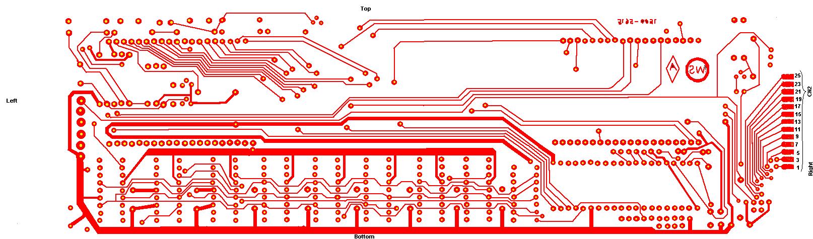
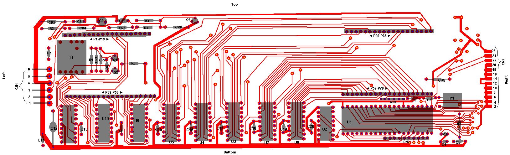
| Pictures |
| Miscelaneous |
| U1-main controller chip |
| Specs |
| U2-hex non-inverting buffer |
| U3-U10-VFD drivers |
| Q1-Q3-caned transistors |
| Y1-resonating crystal |
| T1-Transformer |
| C1,C2-ceramic capasitor |
| C3-tantulum capasitor |
| C4-tantulum capasitor |
| C5,C11,C13-C20-ceramic capasitor |
| C10-ceramic capasitor |
| C12-tantulum capasitor |
| R1-resistor(org,org,blk,gld) |
| C6,C7- ceramic capasitor |
| C8-ceramic capasitor |
| C9-electrolitic capasitor |
| R2-resistor(brn,blk,red,gld) |
| R3-resistor(org,org,red,gld) |
| R4-resistor(grn,brn,red,gld) |
| R6-resistor(brn,blk,org,gld) |
| R7-resistor(brn,blk,brn,gld) |
| RN1- |
| RN2- |
| CR1-CR8-diodes |
| J1-power connector |
| J2-parrallel connector |
| P1-P78-VFD connector pins |
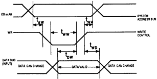
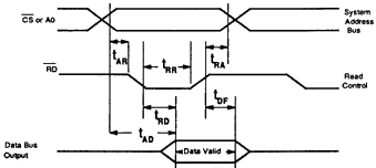
|
CS |
WR |
RD |
A0 |
HOST ACTION |
|
0 |
0 |
1 |
1 |
Write Commands to display |
|
0 |
0 |
1 |
0 |
Write ASCII Data or Control Codes to display |
|
0 |
1 |
0 |
0 |
Read ASCII Data or Cursor Position from Display |
|
0 |
1 |
0 |
1 |
Read Buffer Status from display |
|
1 |
X |
X |
X |
Display is not Selected (Data Lines are Floated) |
|
PIN |
SYMBOL |
DIRECTION |
NAME |
|
J2-1 |
T0 |
Input |
TTL Serial In Self-Test |
|
J2-3 |
CS |
Input |
Device Select |
|
J2-5 |
RD |
Input |
Read |
|
J2-7 |
A0 |
Input |
Address Bit Zero |
|
J2-9 |
WR |
Input |
Write |
|
J2-11 |
DB0 |
Input/Output |
Data Bit 0 (LSB) |
|
J2-13 |
DB1 |
I/O |
Data Bit 1 |
|
J2-15 |
DB2 |
I/O |
Data Bit 2 |
|
J2-17 |
DB3 |
I/O |
Data Bit 3 |
|
J2-19 |
DB4 |
I/O |
Data Bit 4 |
|
J2-21 |
DB5 |
I/O |
Data Bit 5 |
|
J2-23 |
DB6 |
I/O |
Data Bit 6 |
|
J2-25 |
DB7 |
I/O |
Data Bit 7 (MSB) |
|
SYMBOL |
PARAMETER |
MIN |
MAX |
|
tAW |
A0 Setup to WR |
0 |
-- |
|
tWA |
A0 Hold after WR |
0 |
-- |
|
tWW |
WR Pulse Width |
250 |
-- |
|
t DW |
Data Setup to 7WR'- |
150 |
-- |
|
tWD |
Data Hold after-WRK |
0 |
-- |
|
SYMBOL |
PARAMETER |
MIN |
MAX |
|
tAR |
CS, A0 Setup to RD |
0 |
--- |
|
tRA |
CS, A0 Hold after RD |
0 |
-- |
|
tRR |
RD Pulse Width |
250 |
-- |
|
tAD |
CS, A0 to Data Out Delay |
-- |
225 |
|
tRD |
RD to Data Out Delay |
-- |
225 |
|
tDF |
RD to Data Float Delay |
-- |
100 |
| This data sheet is for a different model but it is almost identical to this model except for the demntions and power pinout. |
| Charts were copied from VL-1040-51.html data sheet |
| If anyone has ideas on programing for this display email here: |