1.Interface/Boundary Characterization Using Transmission Electron Microscopy TEM analysis is an importance technique for determining composition and bonding status at surface/interface/boundary areas. It can deliver an atomic number sensitive Z-contrast image by scanning the electron probe on a single atomic column by a single atomic column. In addition, TEM provides us with the information on chemical species and atom sites inside a nanoscaled structure. By combining them with theoretical modeling and structural simulation, it is possible to exactly know crystallographic, chemical and position information at the nano scale.
|
|
|
|
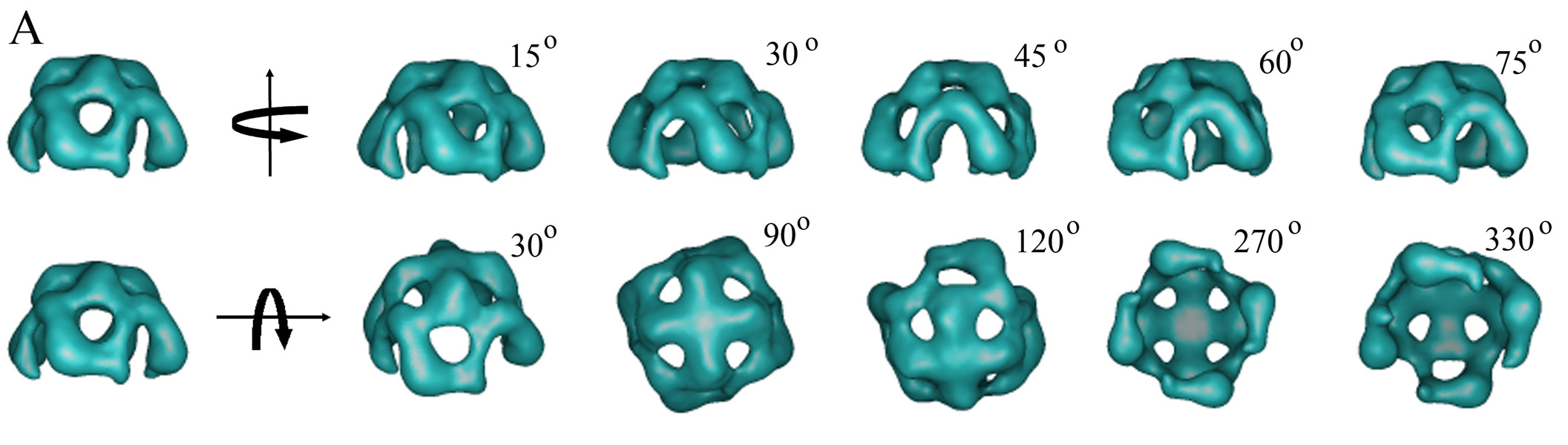
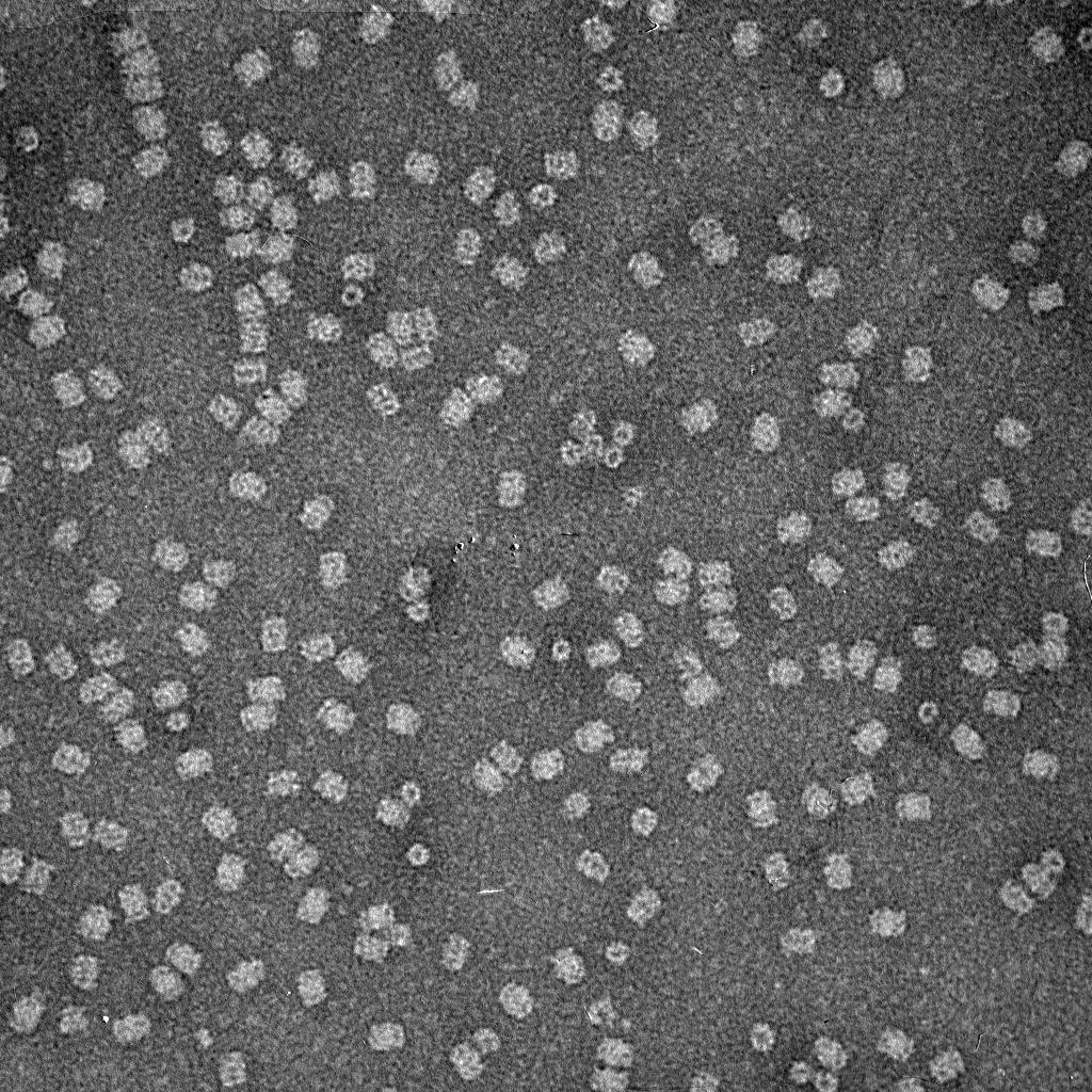
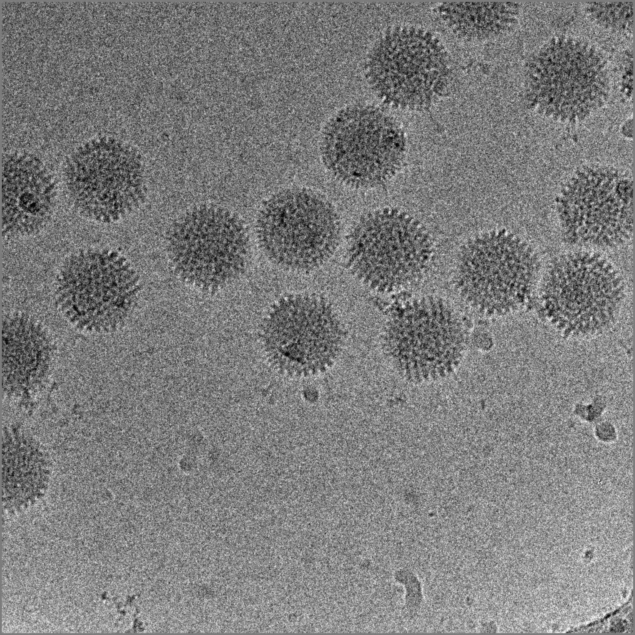
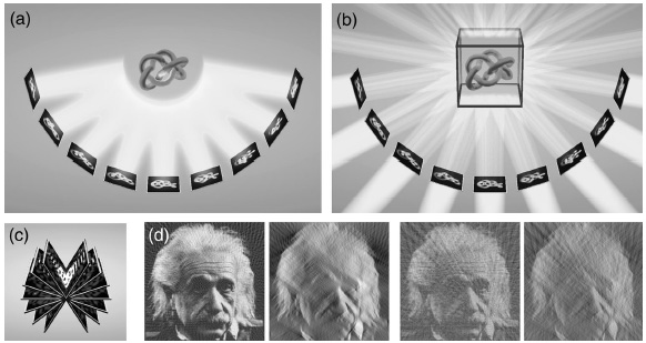
| 2.Negative stainning, Cryo-electron Microscopy and 3D-Tomography Techniques A.Negative stainning B.Cryo-electron Microscopy C.Electron tomography is a new imaging technology, which employs TEM to collect projections of an object and uses these projections to reconstruct the object. |
|
|
|
3.Protein purification and 3D crystal growth A.We try to use 4 columns ( two Ni-columns, one Q-coulmn, and one super200 column) to purify one membrance proteins by FPLC. B.3D crystal
|
|
|
|
image gallery
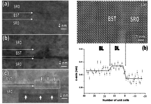
1. Epitaxial SrRuO3/Ba0.7Sr0.3TiO3/SrRuO3 thin film capacitors were prepared on SrTiO3 substrates by pulsed laser deposition. The structures of stacked BST films with different thicknesses
were investigated by transmission electron microscopy. A distinctive layer of about 3 nm of
thickness was identified within BST films thicker than 9 nm at the interface with the SrRuO3 bottom
electrode. The distinctive layer is misfit dislocation-free showing pseudoconstant lattice parameters.
Misfit dislocations are formed at the interface between the distinctive layer and the BST film bulk
layer relaxing the latter as the film thickness increases. The effect of the distinctive layer on the
system dielectric response is discussed within the framework of an interfacial dead-layer model. |
|
J.Q.HE et al. |
|
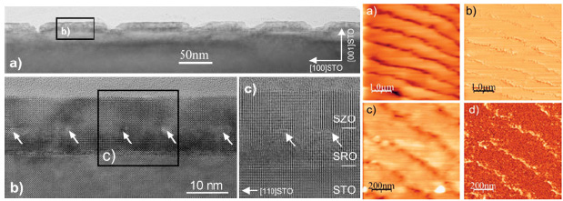
2.At the SrRuO3/LaAlO3 interface a type of dissociated superdislocations in connection with Ruddlesen-Popper type planar defects is found. The dissociated superdislocations involving a (001) RP-defect, {111} stacking faults and their accompanied partial dislocations can contribute to the relaxation of misfit stresses. |
|
3.The SrTiO3 /Si interface was investigated by transmission electron microscopy for SrTiO3 films
grown on s001d Si by molecular-beam epitaxy with different native oxide sSiO2d removal
treatments, and Sr/Ti flux ratios. The interface and film microstructure were independent of the
process used to remove the native oxide, but the interface reactivity was dependent on the Sr/Ti flux
ratio. A low Sr/Ti flux ratio s,0.8d resulted not only in a layer of amorphous material at the
film/substrate interface but also in the formation of crystalline C49 TiSi2 precipitates at that
interface. These results are consistent with thermodynamic expectations in which it is paramount to
maintain separation between TiO2 and the underlying silicon.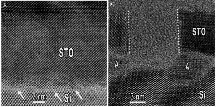 |
|
J.Q. HE et al. |
|
4.The microstructure and the interfaces of HfO2 ?lms deposited by metal-organic chemical vapor deposition directly on
silicon (0 0 1) substrates were investigated by means of transmission electron microscopy. For two different precursors,
Hf(O-i-but)2(mmp)2 and Hf(diethyl-amide)4, electron diffraction analysis showed a gradual transformation from the
amorphous phase to the monoclinic phase in the deposition temperature range of 350�C600C. At an intermediate
substrate temperature, 550C, a small amount of tetragonal second phase was additionally observed. For the two types
of precursors, the thickness of the interfacial amorphous layer was found to depend on the deposition temperature and
showed a major decrease along with the amorphous to crystalline transition of the ?lms. The in?uence of the substrate
surface preparation and of post deposition annealing on the thickness of the interfacial layer is also discussed.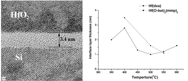 |
|
5.Perovskite La0.7Ca0.3MnO3 (LCMO) thin ?lms were grown epitaxially on SrTiO3 (STO) and NdGaO3 (NGO) substrates by pulsed laser deposition. The microstructure of these ?lms was investigated by means of high-resolution
and Bragg-diffraction contrast transmission electron microscopy. Due to the small lattice mismatch in the system of
LCMO/NGO, the ?lms showed a higher structural perfection than the ?lms on STO substrates. Mis?t dislocations were
not detected over large areas in the LCMO ?lm grown on NGO. In contrast, two types of mis?t dislocations with
Burgers vectors a/0 10S and a/110S were frequently observed at the LCMO/STO interface. MnO precipitates were
identi?ed in the LCMO ?lms by combining energy-dispersive X-ray spectroscopy with electron diffraction analysis. The
MnO precipitates were usually formed in the ?lm away from the film/substrate interface. Their size and density
increased with the film thickness.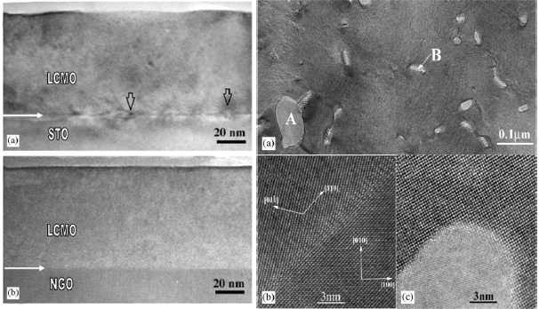 |
|
J.Q. HE et al. |
|
CED-4
|
|
J.Q. HE et al. |
|