formerly
Georg--August--Universität Göttingen, Forschungseinrichtung Röntgenphysik, Geiststraße 11,D--3400 Göttingen, Fed. Rep. of Germany
The optical resolution of zone plates is in the order of the dimension of the outermost zonewidth. Therefore, it is a great challenge to fabricate smaller structures. Inorganic photoresists based on the photostimulated silverdiffusion in chalkogenides, promise some advantages compared to the organic resists used nowadays [1]: high resolution, high contrast, high sensitivity and dry processing. Inorganic photoresists coated with a silvercontaining layer use the effect of photostimulated silverdiffusion. Illumination with photons or electrons of an energy greater 3 eV leads to photoinduced charge separation at the interface. The created photoelectrons migrate into the germaniumsulfide and are trapped near the interface. The very mobile, positive charged silverions follow this potential into the germaniumsulfide. The illuminated, silverdoped germaniumsulfide areas are more stable to alkaline solutions than the undoped areas, so that they can be developed. Before development the remaining silvercontaining layer must be removed to allow the developer to attack the chalkogenide. After development the remaining silverdoped chalkogenide serves as an etch mask for the following structuring processes. These investigations deal with the inorganic resist system silversulfide--germaniumsulfide.
Germaniumdisulfide of high purity was obtained by our cooperators from Sofia, Bulgaria. The Germaniumdisulfide bulk material was thermally evaporated out of amolybdenium effusion cell in a high vacuum of about 2*10-4 Paon chromium coated glass substrates.The used thicknesses varied from 20 nm to 55 nm. These thin GeS2-layerswere sensitized by dipping them into a aquaous silvernitrate solution, leading to a hardly soluble polycrystalline silversulfide layer.For contrast measurements in the visible a grey step-wedge was fabricated by evaporation of chromium steps on a glass substrate.The exposition to visible light took place in a simple optical construction consisting of a halogen lamp and a condenser contact-printing the grey wedge into the resist layers.The exposition to UV-light was done by holographic exposure of the Göttingen MZP3 [2] at a wavelength of 171 nm in immersion.The exposition to weak X-rays took place at the BESSY synchrotron radiation source in Berlin in the "white" light through a 50 nm Cr filter. The electron beam irradiation took place in the scanning electron microscopeat our institute with an ELPHY electron beam lithographic system.
For the desensitization, that means the removal of the not used silvercontaining layer, a concentrated iodine--potassiumiodide solution was taken, solving silversulfide in a potassiumiodide--silver complex. A weak aquaous KOH-solution, with etch rates of about 2 nm/s for undoped germaniumsulfide served as developer.Reactive--Ion--Etching--investigations (RIE) were performed at our institute at a cylindrical reactor with a circular cathode with an area of 50 cm2.The emitter worked at 13.56 MHz with a maximal power of 300 W.Etch gases were: O2, Ar, CBrF3, SF6.
Investigations on the resolution of the resist were done with the MZP3 exposition and with the electron beam lithographic system
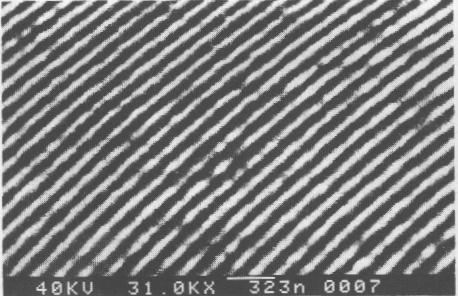
After first not optimised investigations the resolution of the resist could be determined down to 55 nm lines/spaces in the UV ( Figure I) and down to 32 nm lines/spaces with the electron beam ( Figure II). The micrographs still do not show a resolution limit.The sensitivity to visible light of 25 nm thick GeS2 layers is 5 times higher than that for 55 nm thick ones. Absolute sensitivities could not be determined in the visible and in the UV spectral range. The sensitivity to UV-light at 171 nm wavelenght of 24 nm thick GeS2 layers is in the range of that of the organic resist AZ 1350 at a thickness of 45 nm. The contrast reaches a value of up to 7 for expositions to visible light.In XUV--exposition the contrast reaches 16 at a sensitivity of 600 mJ/cm2 for 24 nm GeS2 and 20 at 1100 mJ/cm2 for 47 nm GeS2.In E-beam lithography the contrast reaches 10 at an acceleration voltage of 10 to 20 keV and a sensitivity of 650 µC/cm2 for 3 keV electrons down to 6500 µC/cm2 for 40 keV electrons (all for 24 nm thick GeS2).The RIE investigations show, that a GeS2 layer is a stable mask against an O2--plasma. The etch rates vary from 5.5 nm/min for 5.32 Pa O2-pressure, 580 V selfbias voltage and a power density of 1 W/cm2 down to 0.4 nm/min for 5.32 Pa, 270 V and 0.2 W/cm2. The etch rates for SF6 and CBrF3 are about 90 nm/min for similar conditions. Ar shows an etch rate of about 15 nm/min for 0.7 Pa, 420 V and 0.5 W/cm2.
Figure I:Outermost Zones of MZP 3 in 28 nm GeS2 on Cr
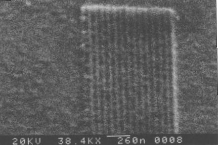
Figure II: 32 nm L/S in 53 nm GeS2 on Cr by 40 eV E-Beam Lithography
The silversulfide/germaniumdisulfide resist system shows high resolution and high contrast with a relatively low sensitivity. It is untoxic compared to other inorganic resists like Ag2Se/GeSex or As2S3. Large substrates can be coated homogenously with a thin resist film in a dry vacuum deposition process. The thin and opaque (to UV and XUV) layers avoid the standing wave effect. The thin layer is stable to an O2-plasma and can serve as a mask in a bilevel resist scheme for the structuring of an organic planarising sublayer.
I like to thank the Stiftung Volkswagenwerk for the founding of this work, BESSY and my collaborators for their help.
This Article was published in: Springer Series in Optical Sciences, Vol.67
X-Ray Microscopy III
Eds.: A. Michette, G. Morrison and C. Buckley
Springer Verlag Berlin Heidelberg 1992
Optimized Result are published in my german dissertation guiding to 18 nm L/S by E-beam-lithography