 |
 |
 |
 |
 |
 |
| Unaxis PECVD (Plasma Enhanced Chemical Vapor Deposition) This tool deposits a layer of oxide or nitride onto the substrate (silicon wafer). |
| Woollam Ellipsometer The ellipsometer checks the thickness of the deposited layer. The center tends to be thicker than the area near the circumference. |
| Spinner/Hotplate The spinner spins a layer of photoresist on the substrate. The hotplate bakes the photoresist. |
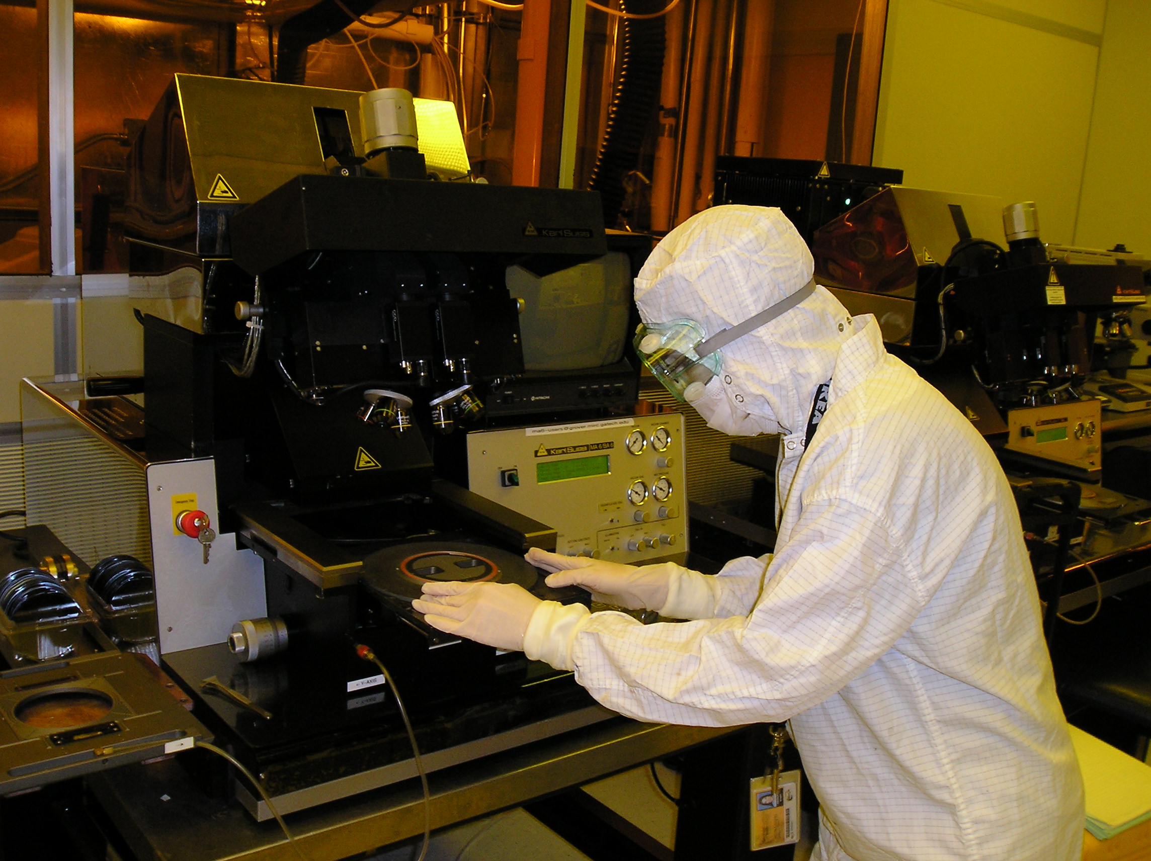
| Karl Suss MA-6 Mask Aligner The photoresist is like film. The mask aligner essentially "snaps a picture," or transfers a pattern from a mask to the photoresist. |
| Developing In order to see the pattern you need to develop it just like photographers do in their dark rooms. Developing removes excess photoresista so that the pattern will appear. |
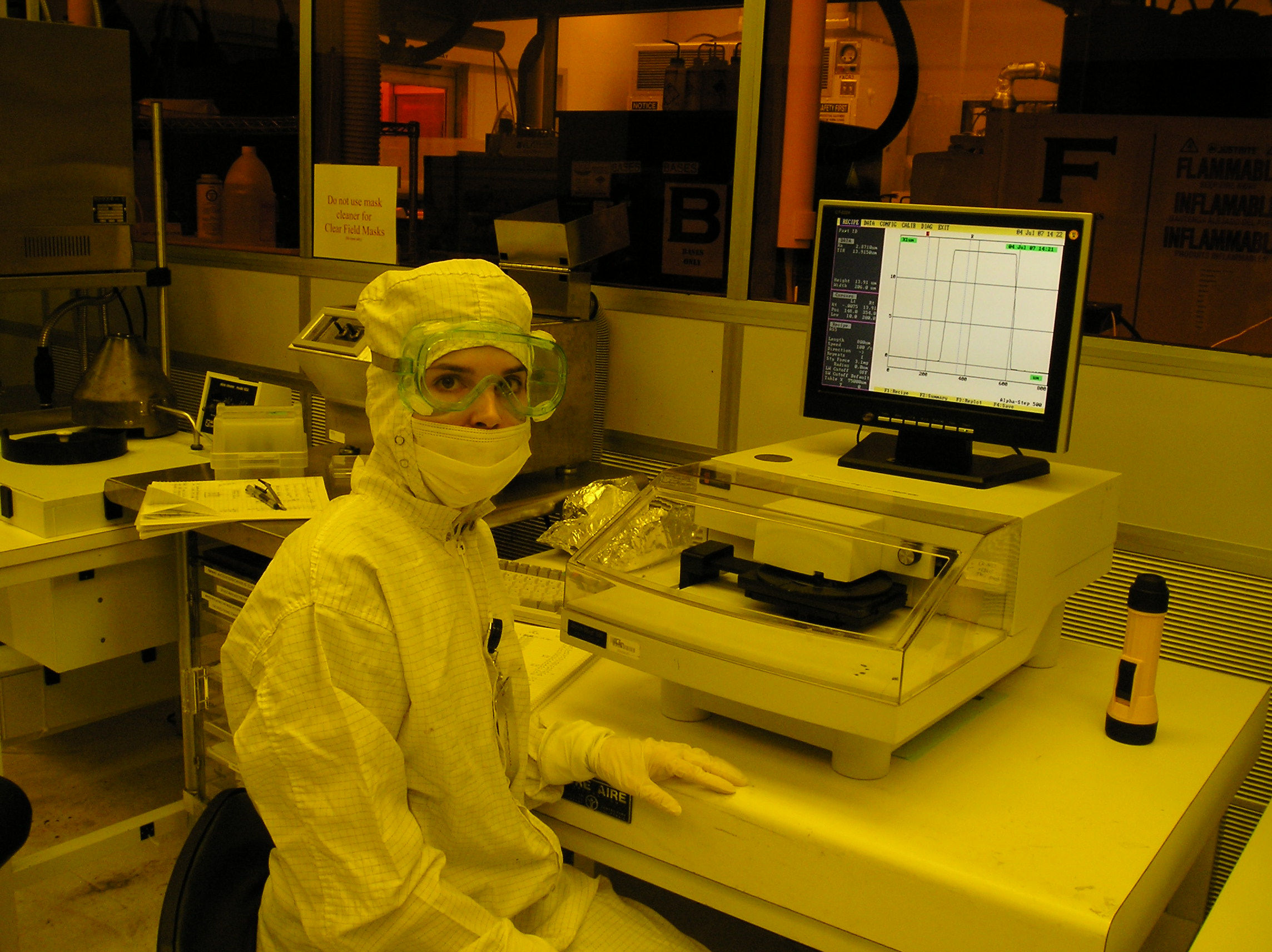
| KLA-Tencor P15 Profilometer The profilometer measures the depth oft he trenches where the photoresist was removed, or the thickness of the photoresist that remains |
| Vision RIE-Oxide (Reactive Ion Etcher) The etcher takes off layers of the surface one cycle at a time. There are two surfaces in this case: the photoresist and the oxide or nitride deposited on the substrate by the PECVD. Each layer is taken off at different rates because each surface has a different chemical makeup, and therefore reacts differently with the gases released by the etcher. |
 |
 |
 |
| Ms. Murray and her new friends spent the summer in the cleanroom at the Microelectronics Research Center. Below is a brief overview of what we did with a description of each tool. Our presentation can be found at: www.mirc.gatech.edu/education/2007_ret.php Go to the bottom of the page and select NNIN RET 2007 ICP Selectivity Profiling |
| Ms. Denny |
| Ms. Hamby |
| Ms. Denny |
| Ms. Denny |
| Ms. Murray |
| Ms. Murray |
| Jaime Z - PhD Student |
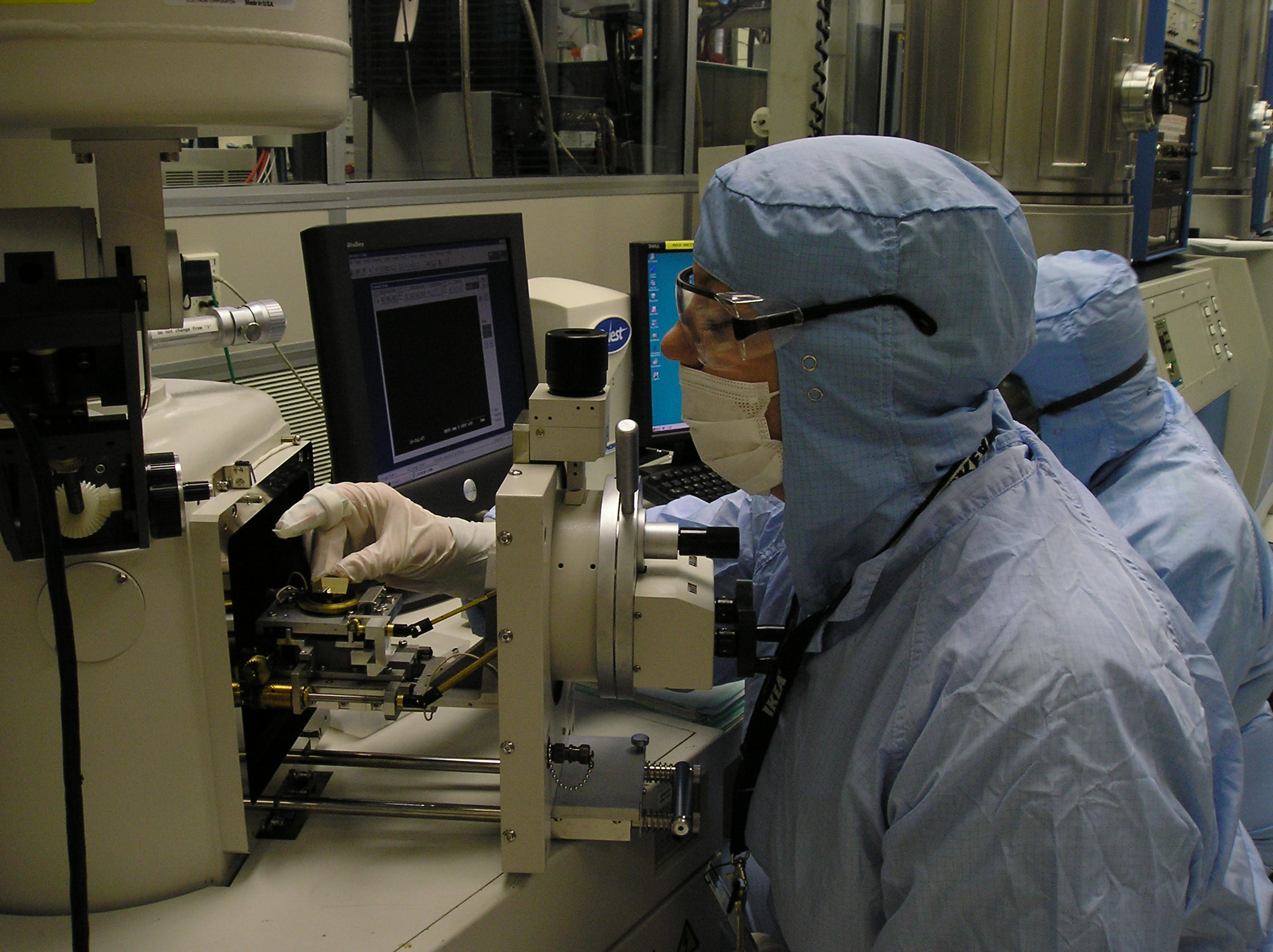
| SEM (Scanning Electron Microscope) |