|
|
|

|
|
||
|
|
Power Supplies |
|
IntroductionA power supply is an essential component in most, if not all, electronic equipment. Most electronic circuits require a power source in order to operate. This power source is usually DC, and is provided by a DC Power Supply. For most electronic equipment, input to the DC power source comes from the sine wave provided by the AC mains, or line voltage. A power supply provides all required power to enable the active circuits to operate. For example a controller requires a source of power so that the signals from a transmitter can be controlled to produce a controlled signal. A power supply can be viewed using the following block diagram. See figure 1.
|
||
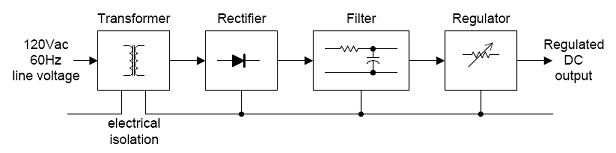
Figure 1. Power Supply Block Diagram
The transformer
Provides isolation, and brings the output voltage to an appropriate level one more suitable for the rest of the circuit. Transformers can either step-down (reduce), or step-up (increase) a voltage, depending on the type of transformer. For most power supplies a step down transformer is used. Typical secondary voltages are 6.3, 12.6, 25, 36, and 48 volts. Most transformers are designed to provide a dual polarity power suppy, and are referred to as Center Tapped (CT), meaning that the secondary has two identical windings.
The rectifier
Converts the ac voltage from the transformer to a pulsating dc voltage. This is normally done with one or more diodes. A diode, is a two terminal device that permits current to flow in one direction only.
Most diodes are identified by a 1Nxxxx designation written on the diode. For example: 1N4001. In many applications four diodes are used together in a bridge configuration, and can be purchased as a single component, in a package with 4 leads.
The filter
The pulsating DC voltage needs to be smoothed. The capacitor is a component that can hold a charge (similar to a tank of water), and convert the pulsating DC voltage to a steady DC voltage with a minimum ripple. The capacitor is the most common component used for power supply filtering, but when large currents are required or in high efficient switching power supplies, inductors are also used.
The Regulator
The regulator maintains the output voltage at a constant value relatively independent of the line voltage variation, load current variation, and temperature changes. This circuit or device is most readily available as a component or an Integrated Circuit (IC).
Rectification (AC to DC)
The basic difference between AC and DC is that with DC, current flows in just one direction; while in AC the current is bi-directional. See Figure 2.
We can convert from AC to pulsating DC by restricting the AC power source to providing current flow through the circuit on only one-half (one polarity) of the sine wave, as shown in Figure 2.
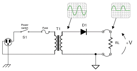
Figure 2. Conversion from AC to DC (positive half-wave rectification)
The method to limit current to one direction, shown in Figure 2, uses the characteristic of a diode that permits current to pass only one way. This is called half-wave rectification of the input sine wave, since conduction occurs on just one alternation (half cycle). The circuit provides current in one direction through the load resistor RL, which increases and decreases with the input AC sine wave voltage.
If the diode is reversed, then the current will only conduct during the negative part of the cycle. See figure 3. In this configuration a negative DC voltage is produced.
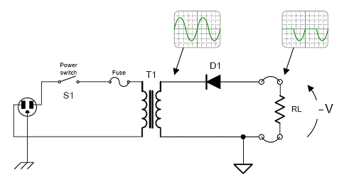
Figure 3. Conversion from AC to DC (negative half-wave rectification)
The two configurations can also be combined, providing both a positive and negative DC voltages. See figure 4.
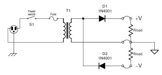
Figure 4. Conversion from AC to DC (bipolar half-wave rectification)
Full Wave Rectification
A circuit that allows current through the load on both alternations of the input sine wave is illustrated in Figure 5. On one alternation (half cycle) of the input AC sine wave, the top end of the transformer has a positive voltage and the bottom end has a negative voltage relative to the center tap (common).
All waveforms are measured with respect to the center tap (common) of the transformer.
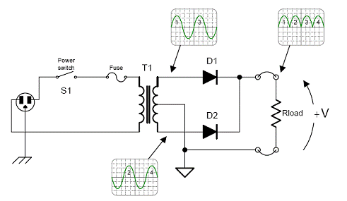
Figure 5. Conversion of AC to DC (positive full-wave rectification)
On the next alternation, the top of the transformer becomes negative and the bottom end goes positive. When the voltage at the top of the transformer is positive, diode D1 conducts and provides current through the load resistor and back through the center tap of the transformer. At this time, however, the bottom end of the transformer is negative, and diode D1 is reverse biased and contributes no current to the load. On the next alternation, since the bottom end of the transformer is positive, D2 conducts providing load current and D1 is now reverse biased. Both rectified alternations appear across the load as pulsating DC.
The current path, when each diode conducts, is through the diode, then the load, and back through the center tap of the transformer. Notice that only one-half of the transformer is used for each alternation and therefore the voltage developed across the load is one-half the total transformer, secondary peak voltage minus one diode drop.
Again if the diodes are reversed, a negative DC voltage is produced. See figure 6.
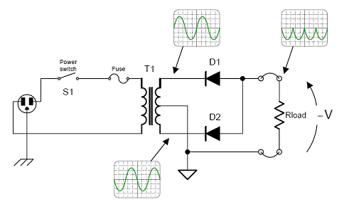
Figure 6. Conversion of AC to DC (negative full-wave rectification)
The two configurations can also be combined, providing both a positive and negative DC voltages. See figure 7.
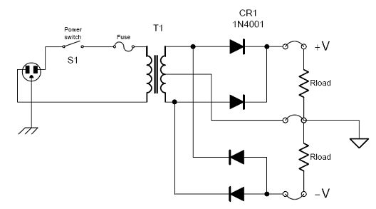
Figure 7. Conversion of AC to DC (bipolar full-wave rectification)
Bridge Rectification
A full-wave rectification method that provides the total transformer voltage across the load and also eliminates the need for a center-tapped transformer is shown in Figure 3. Four diodes are required in this configuration connected as a "bridge". When the top end of the transformer is positive, D1 conducts and current (+i) flows through the load and back through D3 to the bottom end of the transformer. On the next alternation, the bottom end of the transformer is positive and current (-i) flows through D2, the load, and through D4 back to the top end of the transformer.
Because it provides current to the load on both alternation of the input sine wave, and doesn't need a center-tapped transformer, the bridge type is the most common method of power supply rectification. The four bridge diodes are usually sealed in a single package with four connecting leads.
Note: When taking measurements using the scope, the output trace is referenced to the Load GND, but the input to the bridge should be measured across the secondary of the transformer, and not referenced to the Load GND.
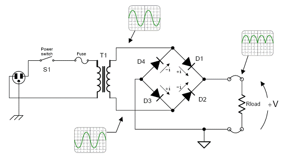
Figure 8. Conversion of AC to DC (full-wave rectification using a Bridge)
Filtering
The voltages developed across the loads in the rectification circuits we have just described, are not the same DC as provided by a battery, but are time-varying pulsating DC voltages. The average DC component of this waveform, is 0.637 of the peak value for a full wave rectifier and 0.318 for a half wave rectifier. There is as well as a large time varying component we call ripple.
To make a DC power supply more like a battery requires that we reduce the ripple component. We can do this with a filter capacitor (see Figure 9).
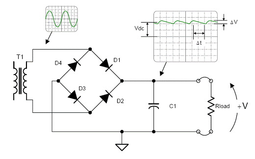
Figure 9. Capacitive filtering and operation
This capacitor will maintain the output voltage near the peak value even when the input voltage drops to zero. It does this by storing charge and providing the load current when the AC input voltage from the transformer is less than the required DC output.
We can get a feel for the operation of a filter capacitor by analyzing the circuit of Figure 9. For simplicity, a full-wave rectifier is shown, but the same theory applies to a half-wave rectifier.
In Figure 10, the input that the capacitor would see is superimposed on the output wave, with two vertical lines indicating the time interval the diode is conducting and charging the capacitor. The capacitor charges to the peak of the input waveform minus the voltage across the diode (0.7V).
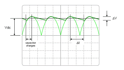
Figure 10. Capacitive filtering and operation enlarged view
The voltage waveform across the capacitor shows the charging and discharging of the capacitor.
Discharging results from load current flowing from the capacitor during the time the diode is not conducting, and this causes the capacitor voltage to drop by an amount DV. We will assume that the peak voltage across the capacitor is equal to the DC output voltage (Vdc = Vp). This assumption is good because the ripple voltage DV should be much smaller than the Vp or Vdc.
A more accurate approximation for Vdc would be: (![]() ) as shown with the dotted line.
) as shown with the dotted line.
Ideally, to have pure DC at the load resistor, DV would be zero. But this would require an infinite size filter capacitor. The relationship between the ripple DV and the size of capacitor required can be calculated as follows.
The basic capacitor equation is
![]()
Where q is the charge on, and V the voltage across, the capacitor. During discharge, we assume the capacitor loses an amount of charge Dq during the time interval Dt as a result of current flowing through the load. Further, assume the load current is constant over this time (Dt) since he DC voltage change DV is too small to affect the current. We can determine the voltage change DV (ripple) across the capacitor by dividing the basic capacitor equation by the increment of time Dt.
![]()
but ![]() the
current
the
current
so ![]()
Solving for DV which is the peak-to-peak ripple we get
![]() again,
provided DV << Vdc
again,
provided DV << Vdc
Since the current I is the independent variable determined by the load resistor, the ripple DV is inversely proportional to the size of the capacitor. The capacitor discharge time Dt is roughly 8 ms for the full-wave rectification circuit of Figure 9.
Actually, the ripple repeats at 8.33ms or ![]() Hz for full-wave rectification and
Hz for full-wave rectification and
16.67 ms (![]() Hz) for half-wave
rectification. We normally assume that the capacitor charges during the 0.33ms
or 0.67ms.
Hz) for half-wave
rectification. We normally assume that the capacitor charges during the 0.33ms
or 0.67ms.
Example:
Find the ripple voltage DV for a half-wave rectified power supply if the load current I is 100mA and C is 1000mF.
Dt = 16ms for half-wave rectification
With C = 1000mF
![]() 1.6V
1.6V
note that if the value of C is too small, meaning the ripple voltage is too large, we obtain incorrect results.
For example if C=100mF we would get:
![]() 16V which is clearly
impossible. In this case the capacitor is not sufficiently large to hold the
charge, for the specified load.
16V which is clearly
impossible. In this case the capacitor is not sufficiently large to hold the
charge, for the specified load.
Find the ripple voltage DV when the capacitor C is increased from 1000mF to 2000mF.
then ![]() 0.8V
0.8V
We can see from this example that if we doubled the capacitor size, the ripple voltage would be half the voltage and the lower the ripple, the better.
Since for full-wave rectification the capacitor discharges only for 8ms before it is recharged, the capacitor size required for a given load current and ripple voltage is one-half the size of that required for half-wave rectification.
Example:
Find the ripple voltage DV for a full-wave rectified power supply if I is 100mA and C is 2000mF.
Dt = 8ms for full-wave rectification
with C = 2000mF
![]() 0.4 V
0.4 V
These results show why half-wave rectification is rarely used. It requires twice the capacitor value to obtain the same ripple voltage.
Complete Power Supply
We have looked at the basic elements of a power supply. Now we will consider a practical power supply circuit. Figure 11 shows the power supply configuration we shall study. Notice that a full-wave bridge configuration is used for rectification. Again, a full-wave rectification circuit has the advantage of less discharge time for the filter capacitor, ie, smaller capacitor; also, we don't need a center-tapped transformer with the bridge configuration.
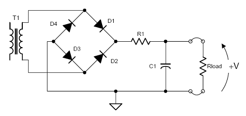
Figure 11. Power Supply
The DC output voltage (Vdc) for this bridge circuit is the peak value of the input voltage Vp minus two diode drops of 0.7V, or
![]() recall
recall ![]()
A resistor R1 has been added between the diodes and the filter capacitor. The purpose of this resistor is to limit the diode surge current to a safe value when power is first turned on, since the capacitor, having no charge on it, looks like a short circuit. R1 is selected to keep the surge current I below the one cycle surge current rating of the diode. For a diode that has a maximum forward current rating of lA, the surge current rating is 30A; a 2A diode has a surge rating of 60A and so on. See the specification sheet of a rectifier diode like the 1N4004.
In many instances the DC resistance of the transformer, which is the secondary winding resistance and also the reflected primary resistance (changed by the square of the turns ratio), is sufficient to limit the current to below the diode surge current value. This must be taken into account when R1 is calculated.
Example:
Find the required value of R1 (figure 11 ) for a power supply if the peak capacitor voltage Vp is 20V, the effective DC resistance of the transformer Rx is 0.07 W, and a 3A bridge rectifier is used.
![]()
For a 3A bridge rectifier, Ip is 90A.
then ![]()
and ![]()
Rectifier Diode Reverse Voltage Rating
If we assume that the filter capacitor in Figure 10, charges to its positive peak of the transformer secondary AC voltage waveform (neglecting the 0.7V diode forward drops), then when the input waveform swings to the negative peak, there will be a reverse voltage of 2Vp across the rectifier diode, i.e., +Vp on the diode cathode and -Vp on the diode anode. The rectifier diode should have a high enough peak inverse voltage (PIV) rating to with-stand the reverse voltage it will encounter in the powers supply circuit. To be conservative and accommodate AC line voltage spikes that can pass through the transformer, it is a good idea to use a diode with a PRV rating of at least twice the value of 2Vp, or in other words 4Vp.
Example:
Find the required peak reverse voltage (PRV) rating for the diode bridge of Figure 11 if the capacitor voltage Vp is 25V.
If we neglect the rectifier voltage drops and assume that Vc is equal to Vp, then the input waveform can swing to -25V. This means the rectifier diodes can see a peak reverse voltage rating of (2´25V) or 50V. To be conservative, we would use a bridge with a PRV of 100V.
Example:
For the power supply of Figure 11, we require a DC output voltage of 16V, maximum, a current of 500mA, and a maximum ripple of no more than 5%. Find the transformer rating, diode rating, R1 if the effective transformer DC resistance Rx is 0.l W, and the required capacitor size.
If we rearrange equation
![]()
we get ![]() Vrms
Vrms
We could then use a standard 12 V or 12.6 V transformer.
To be conservative, we shall double our 500mA load current and use a 1A transformer and also a 1A bridge rectifier rated with a minimum PRV of four times Vc or 64V (we shall use a standard size 100V PRV bridge).
When power is first turned on, we could have the maximum voltage of 16V driving current into the uncharged filter capacitor, which appears as a short circuit. With a 1A bridge, the specified surge current Is is 30A.
So ![]()
Since Rx is given as 0.1W, Rs is 0.43W.
The ripple voltage is 5% of 16V or 0.8V, so the required filter capacitor is:
![]() mF
mF
A standard value would be 4700mF.
Power Supply Regulation
If the input line voltage to our power supply is lowered, the DC output voltage would also drop proportionally. The problem with this simple type of power supply is that the output DC will change with both the input line voltage and the load. Increasing the load current will cause a increase in voltage drop across the diode rectifiers; but a more pronounced voltage drop can occur from the DC resistance of the transformer and the surge resistor R1.
Example:
Calculate the output voltage from a nominal 18V DC power supply with Rx + R1 =1.5W if the load current changes from 200mA to 500mA. Also find the new output voltage with a load current held at 200mA, but the line voltage increases by 10%.
Neglecting the change in the diode drop, the voltage drop DV for the 300mA increase in current is:
![]() = 300m ´ 1.5 = 0.45V
= 300m ´ 1.5 = 0.45V
The output voltage with the 500mA load is now
Vdc = 18 - 0.45 = 17.55V
The change DV from our nominal 18V output if the line voltage increases by 10% is:
DV = 18V ´ 0.1 = 1.8V
Our new output voltage is then
Vdc = 18 + 1.8 = 19.8V
We could have obtained the same result by multiplying our nominal value by 1.1. For 10% low line we multiply Vdc by 0.9.
Regulation of a power supply is defined as the change in output voltage (DVdc) due to a change in the load current, or line voltage, divided by the nominal output voltage (Vdc).
Mathematically: Power Supply Regulation = ![]()
This is usually expressed in % regulation as follows:
% Reg. = ![]()
The lower the percent (%) regulation, the better the power supply.
Load regulation is defined in terms of the voltage change that occurs at the power supply output when the load current goes from no load (zero amps) to the full load condition. Manufacturers of regulators also specify some minimum load current to ensure that the output transistors are at their proper operating bias point.
Line regulation is defined in terms of the voltage change that occurs at the power supply output when the input AC line voltage is increased or decreased by 10 percent.
Example:
Find the percent load regulation for a nominal 12V output power supply if the output voltage decreases to 11.9V when the load current is increased from no load to full load.
The change in output voltage is 12 - 11.9 = 100mV
% Load Reg. = ![]() %
%
For the same power supply, find the line regulation if the output voltage drops by 50mV when the input line voltage drops 10 percent.
% Line Reg. = ![]() %
%
Zener Voltage Regulation
A voltage regulator will reduce the effect of load and line variations on the output voltage. The simplest type of regulator uses a zener diode, as shown in Figure 12. This type of regulator uses the fact that the voltage across a zener diode is fairly constant when the current through the device changes.
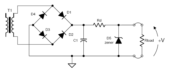
Figure 12. zener diode voltage regulation
Notice the zener diode (or regulator) is added to the output of our basic supply and consists of the zener diode and a voltage dropping resistor Rd.
Selection of the voltage dropping resistor Rd is
based on providing enough current for the zener to operate (![]() ) under all required conditions
) under all required conditions
The least current the zener will conduct is at the 10% low
AC line (LL) voltage and with full load current (![]() ),
Under these conditions, the current through Rd will be
),
Under these conditions, the current through Rd will be
![]()
so ![]()
The zener voltage is selected to equal the desired output voltage from the power supply and so
![]()
The power rating of the zener is selected to handle the
current at the 10% high line (HL) voltage condition with the load
disconnected. (Note: ![]() occurs with the
load disconnected because all the current through Rd must now go through
the zener diode.)
occurs with the
load disconnected because all the current through Rd must now go through
the zener diode.)
In equation form
![]()
but ![]()
Then ![]()
Example:
The required output from a zener-regulated power supply is
9V with a maximum load current of 40mA. If the nominal voltage at the filter
capacitor ![]() is 16V, and the minimum
zener current is l0mA. Find the voltage and power rating of the zener, the
required value of Rd , and also the required power rating of Rd.
is 16V, and the minimum
zener current is l0mA. Find the voltage and power rating of the zener, the
required value of Rd , and also the required power rating of Rd.
First, we can find the value of Rd , remembering that
![]() is the capacitor voltage at low
line voltage and is equal to
is the capacitor voltage at low
line voltage and is equal to ![]() (90%
of
(90%
of ![]() ).
).
![]()
We can use a standard 100W resistor value – a lower value is more conservative.
For the power rating of the resistor Rd, we need to
find the total current at high line voltage. Again remembering that ![]() is the capacitor voltage at high
line voltage and is equal to
is the capacitor voltage at high
line voltage and is equal to ![]() (110%
of
(110%
of ![]() ).
).
![]() mA
mA
then ![]() W
W
To be conservative, we should use a 2W resistor.
The voltage rating of the zener is simply the required
output voltage of 9V. We will use a standard zener value of 9.lV. For the
power rating of the zener, we simply multiply the maximum current ![]() through Rd (at high line)
by the zener voltage rating.
through Rd (at high line)
by the zener voltage rating.
![]() W
W
To be conservative, we should use a 2-watt zener.
The voltage across a zener diode changes slightly with the current through the zener diode because of the zener resistance Rz. The actual voltage rating for a zener is specified at a given test current and consists of the zener breakdown voltage plus the voltage drop across the zener impedance.
Example:
Determine the zener current ![]() at
maximum load and the % load regulation for the previous example. Use a lN4739
(9.1V) zener that has a zener impedance Rz of 5W at a test current of 28mA.
at
maximum load and the % load regulation for the previous example. Use a lN4739
(9.1V) zener that has a zener impedance Rz of 5W at a test current of 28mA.
The current Id through Rd is
![]() mA
mA
With a maximum load current of 40mA, the zener current ![]() is
is
![]() 29mA
29mA
The zener voltage (![]() )
with this current, which is close to the specified value of 28ma, is 9.1V. If
the load current goes to zero, all 69mA (Id) will flow through the
zener. The new no load zener voltage
)
with this current, which is close to the specified value of 28ma, is 9.1V. If
the load current goes to zero, all 69mA (Id) will flow through the
zener. The new no load zener voltage ![]() will
be
will
be
![]() 9.305v
9.305v
The zener voltage change ![]() from
no load to the maximum load condition is
from
no load to the maximum load condition is
![]() V
V
The percent load regulation is
% Load Reg. = ![]() %
%