
|
Presented by: Only On Saturday Night
This is the IdeZilla Prototype.
It is a one chip IDE interface to a coco-3 (or any coco).
It has 3 pins for address selection. It can select any block of 11 consecutive addresses from $FFx0 to $FFxA. The "x" being anywhere from 0 to 7. Alternate registers $3F6 and $3F7 are mapped into $FFx9 and $FFxA respectively. The addresses from $FFxB to $FFxF are unselected and unused.
There is also a jumper to reverse the IDE registers from normal.
I use this option in this NitrOS9 LBA-MODE driver
or this CHS-MODE driver.
Circuit board is about 4.6 x 3 inches, see on IDE PCB button.
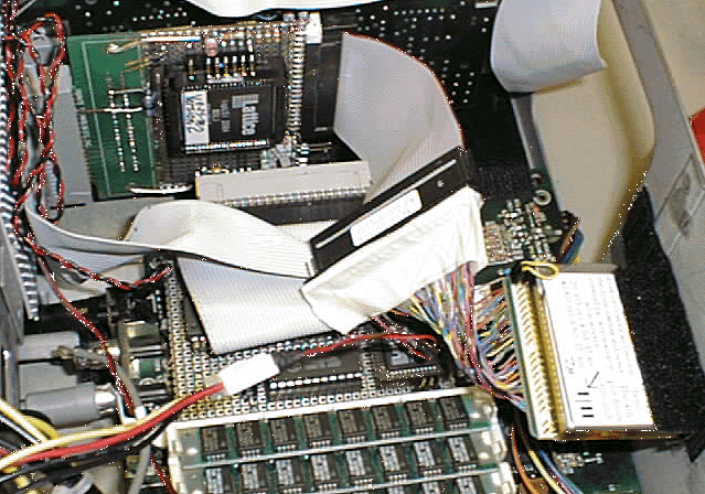
What you see in the photo: A piece of "holey" board with the Lattice
chip mounted, mated to a piece of card edge connector for the gold fingers.
All plugged into a coco extension cable, with card edge connectors as part
of the cable. The card edge connectors glued to the inside of the repack
case. Behind the IDE board is the floppy controller board, then a sound
board. A Kittyhawk (20MB) IDE drive using LBA mode, velcro'd to the side
of the repack case.