|
| Presented by: Only On Saturday Night |
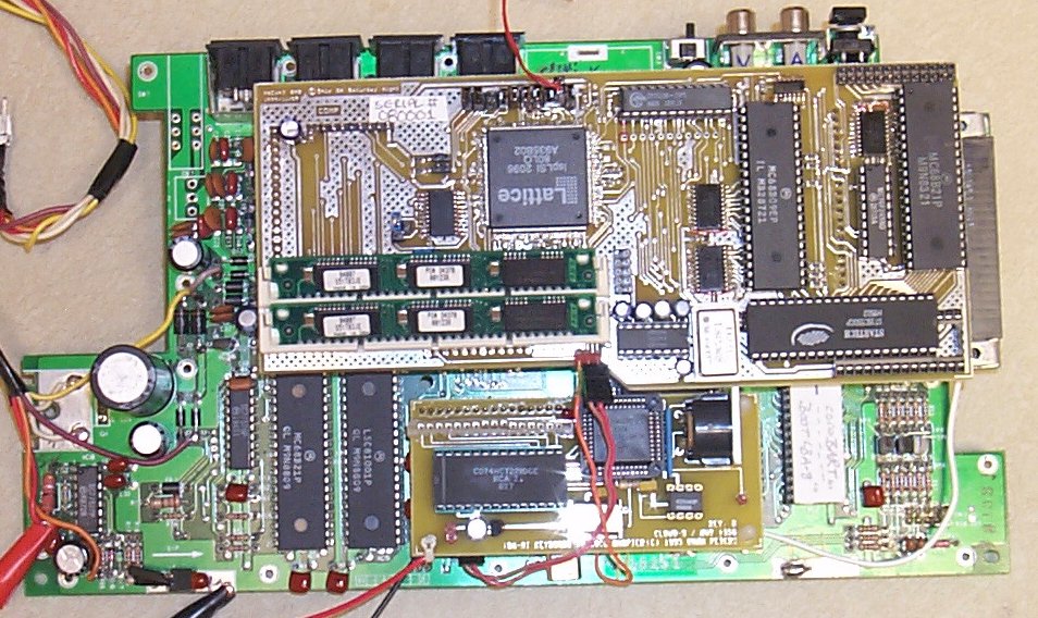
A NoCan2 has been re-wired and the PLD is re-compiled and the two each 1MB DRAM sticks were exchanged for two each 4MB DRAM sticks, 8MB! It's entirely possible and already done! In fact, all of the memory has now been tested, and passes!
NoCan3 Circuit
Board Layout!
Notes by
Robert Gault
| $FF9B: | 76543210
|||||||| |||||||`.. 1MB Video Bit0 (1MB) ||||||`... 2MB Video Bit1 (2MB) |||||| |||||`.... Video Bit2 (direct) ||||`..... Video Bit3 (direct) |||`...... CPU Bit2 (sram) ||`....... CPU Bit3 (sram) || |`........ Page Bit 0 `......... Page Bit 1 |
This was my first choice.
A board wired this way, exists. Tested 11/12/1999 The 1MB, 2MB & 8MB access. |
| $FFAx: | 76543210
|||||||| |||||||`.. Standard GIME Access ||||||`... Standard GIME Access |||||`.... Standard GIME Access ||||`..... Standard GIME Access |||`...... Standard GIME Access ||`....... Standard GIME Access || |`........ CPU Bit0 (sram, 1MB) `......... CPU Bit1 (sram, 2MB) |
The 1MB & 2MB access. |
Currently tested;
Software "MemTest" and "VidTest" written by Robert Gault.
Thanks Robert!
"VidTest.BIN" and "MemTest.BIN" for 6309's are now available at http://home.wwdb.org/irgroup (now at www.geocities.com/idezilla)
To use CPU paging:
1. Disable interrupts.
2. Read the single $FFAx, the single page to update.
3. Write $FF9B with the CPU data for the single $FFAx
page.
4. Write back the single $FFAx, the page to update. This
write puts the CPU bits into SRAM.
5. Write $FF9B with previous CPU bits,
else the next write access to $FFAx
will write the two MSB's of page data wrongly.
6. Enable interrupts.
Now that single page has it's upper 2 bits in that page's
SRAM address.
Note: Every write to a single $FFAx will write the current
$FF9B CPU bits to that single $FFAx location.
To use VIDEO paging:
1. Disable interrupts.
2. Write $FF9B with the data.
3. Enable interrupts.
How it's connected:
The two VIDEO bits are just latched
and then go directly to creating Address A10.
The two CPU bits go to the SRAM
inputs addressed for $FFAX and return to create Address A10.
Whenever a write to $FFAx is needed
the two MSB's are first written to $FF9B, then to $FFAX
then $FF9B is restored to the previous
setting. If it is not restored, the next write to any $FFAX
changes that locations two MSB's.
Additional Note:
I have added a jumper to select
whether the CPU bits go through SRAM or just tie directly.
This will allow users to go directly
to any page, and still have access to $00FFEX vector paging.
On Paul's system, each MMU address selects a standard $2000 block of
RAM. Since the MMU registers are 8 bit lines they only address
$FF*$2000 or $1FE000. The address needs to be extended for two more
bits at $FF9B to get $400*$2000 or $800000. Here is how I would
describe the system.
1) The video bits (xxmmvvvv) at $FF9B have immediate effect and are
used in conjunction with the video offset registers $FF9D-$FF9E. The
combined registers create a pseudo 20 bit register. This enables
access to 1,048,576 (2^20) video offset locations. Since the offsets
are separated by 8 bytes, this covers 8* 2^20 = 8,388,608 (8Meg).
2) The memory bits (xxmmvvvv) at $FF9B have no effect until a value
is sent to an MMU register, $FFA0-$FFAF. When a value is sent to an
MMU register, the memory bits at $FF9B combine with the MMU register
to create a pseudo 10 bit register. This enables access to 1024
(2^10) MMU blocks for a total memory of 1024*8192=8,388,608 (8Meg).
3) The value at $FF9B is latched and therefore stable but is write
only as are the two high bits in the MMU registers.
Paul is able to run OS-9 Level II on the system, but I believe he
needed to change the manner in which the memory bits were processed.
There are more details on his web page describing how to keep the
DRAM at $xFExx constant.
It was a real challenge to write code for this system without having
the hardware for testing. However, the programs were valuable as
they permitted Paul to determine that two bits of the Lattice CPLD
schematic were reversed. Reprogramming resulted in contiguous memory
as
indicated by the Vidtest program.